Designing a low-power embedded product starts with careful component selection from the very beginning. Choosing energy-efficient components, arranging them to minimize energy consumption, and configuring them properly all play a role in the final power budget.
In this topic, we will look at the common components found in a typical Bluetooth LE product and understand how each one affects power consumption. A key point to remember: idle current matters just as much as active current. A Bluetooth LE device spends most of its time sleeping, so even small amounts of current drawn during idle periods can easily add up quickly and can dominate your power budget. Knowing the current draw of each component, both when active and when idle, will help us estimate the overall power budget across different operating modes.
1. Wireless SoC
At the core of every Bluetooth LE device is a wireless SoC that provides both the computational processing capabilities and the radio. The wireless SoC plays a crucial role in the device’s overall power consumption.
You can think of the wireless SoC as a microcontroller + a 2.4 GHz radio. The microcontroller provides the CPU and commonly used peripherals, such as UART and ADC. The rule of thumb here is to select an SoC that offers the lowest CPU processing current, the lowest TX and RX current when the radio is transmitting or receiving, and the lowest power consumption in sleep mode. Below are the numbers for the nRF54L15 SoC:
Value depends on device configuration (memory retention, etc. ) Voltage: 3 V
A key rule for achieving low power, which we will explore in lesson 4, is to configure the Wireless SoC so the 2.4 GHz radio (RX/TX) is ON as infrequently as possible and the CPU is asleep as frequently as possible.
Definition
TX power (dBm): The strength of the radio’s transmitted signal, measured in dBm (decibels relative to one milliwatt). Higher TX power increases range but also increases current consumption. 0 dBm = 1 mW.
PHY (Physical Layer): Defines the data rate and modulation scheme used for the radio link. Bluetooth LE supports multiple PHYs – 1 Mbps (LE 1M), 2 Mbps (LE 2M), and Coded PHY (long range). The chosen PHY affects both throughput and power consumption, since faster PHYs reduce radio-on time per packet.
2. Sensors and actuators
Bluetooth LE devices often include sensors and actuators. The sensor or actuator type depends on the device’s application. Typical sensors in a Bluetooth device include:
Environmental: Temperature, humidity, pressure, air quality
Typical actuators found in a Bluetooth device include:
Haptic: Vibration motors.
Audio: Buzzers, speakers.
Mechanical: Servo motors, small relays.
When aiming for low-power design, it is important to select sensors and actuators that not only have low active current, but also, it is extremely important for them to have low sleep current. As low-power Bluetooth LE devices should be idle 95-99% of the time.
Here are the top guidelines when selecting/configuring sensors
Prioritize sleep/standby current. Bluetooth LE devices spend 95%+ time sleeping.
Use asynchronous (interrupt-driven) sensor operations when applicable (Wireless SoC sleep until data ready).
Avoid fragmented wakeups: Aim to batch sensor events so the system wakes up fewer times. A single long sleep is far more energy‑efficient than many short sleeps, because each wakeup carries additional power overhead.
Avoid activating actuators or sensors during radio TX/RX to prevent high current peaks that reduce battery life. High current peaks with long duration, drastically impact battery capacity.
Use sensors and actuators with operating voltage ranges matching the battery voltage or device PMIC output to avoid needing extra components, or extra voltage rails.
Use lowest acceptable sampling rate for sensors.
Use power-saving schemes implemented by the sensor.
If the device has multiple sensors, group them in a separate power domain on the PCB with dedicated switches to shut off completely when unused.
Consider the values of the pull-up and pull-down resistors for sensors.
Below are typical power consumption values for low-power accelerometer sensors to provide perspective on their current use:
Metric
Value
Unit
Active current@ 100 Hz
0.5 – 700
µA
Sleep/Standby current
0.1 – 10
µA
Shutdown current
0.01 – 2
µA
The current numbers vary depending on the type of accelerometer used, especially in terms of accuracy, resolution, bandwidth, and advanced features included.
3. User interface
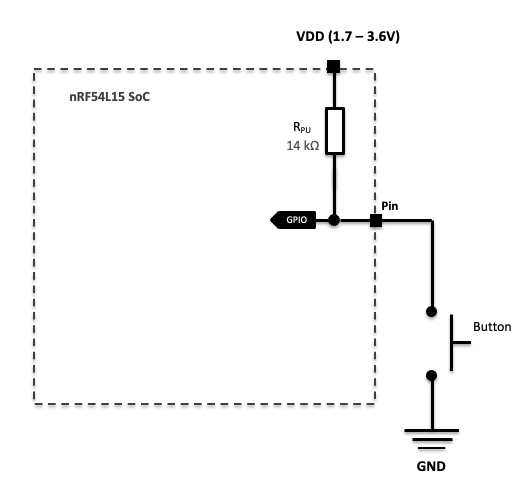
The user interface type selected for a Bluetooth LE device significantly affects its power budget. Some interface devices, such as push buttons, consume low power. When the button is inactive, it draws zero current (As we mentioned before, this current dominates the device’s operating time). When activated, it draws a small current equal to the input voltage divided by the GPIO pull-up resistance. The active current occurs rarely during the device’s lifetime(only when the button is pressed). The table below shows the current of a push button connected as an active low push button through the nRF54L15 14 kΩ Pull-up resistor:
Active-low push button through the nRF54L15 14 kΩ pull-up resistor
Metric
Value
Unit
Condition
Active current
121 – 257
µA
Using internal pull-up resistor of 14 KΩ
Inactive current
0
µA
Active low push button
When we compare mechanical push buttons with capacitive touch buttons, capacitive touch buttons require continuous current even when not being activated. This is fundamentally different from mechanical push buttons. Meaning this is a current that will always be consumed regardless of the device mode of operation.
Metric
Value
Unit
Condition
Active current
1 – 50 µA
µA
Depending on scan rate and method
Inactive current
1 – 50 µA
µA
Depending on method
From a power consumption perspective, the mechanical push button is more efficient than the capacitive touch button because it draws no current when idle, which accounts for 95-99% of the device’s operating time.
Now let us see what happens if the device includes a display. A single LED turned on can consume as much power as the entire wireless SoC when its radio is active.
Incorporating a display into your product drastically increases the power budget and significantly influences battery selection, as most displays introduce both high inactive and active current that depends on size and resolution. The exception is E-Paper displays, which consume zero inactive current even when displaying static content, and only consume current when updating the display content; however, their low refresh rate suits static content only or content that change infrequently. Below are rough estimates of power consumption for small-size common display technologies:
Display Type
Updating Content
Maintaining Static Content
Power When Off
E-Paper
5-20 mA (during refresh)
0 µA
0 µA
Segmented LCD
1-3 µA
1-3 µA
~0 µA
Memory LCD
50-200 µA
5-10 µA
~0 µA
PMOLED
8-20 mA*
8-20 mA*
~0 µA
AMOLED
30-100 mA*
30-100 mA*
~0 µA
TFT LCD
40-100 mA
40-100 mA
2-8 mA
Small LED Matrix
20-80 mA* **
20-80 mA*
0 µA
*Same value because power depends on content brightness, not whether it is changing
** depends on matrix size
In another context, How much current does it cost to keep showing something on a display?
E-Paper ▏ 0 µA Segmented LCD ▎ 1-3 µA Memory LCD ▍ 5-10 µA |─────────── µA/mA boundary ───────────| PMOLED ████ 8-20 mA LED Matrix ██████ 20-80 mA AMOLED ████████ 30-100 mA TFT LCD ██████████ 40-100 mA
Remember: a single LED can draw 5 mA to 20 mA, equal to or exceeding the entire wireless SoC’s current during radio transmission.
Keeping an indication LED on, even with a low blinking frequency, during device sleep significantly increases power consumption and drains the battery. Therefore, it’s highly recommended to turn any indication LED off when the device is in sleep mode.
4. PCB, passives, and 2.4 GHz antenna
The PCB layout, RF passive components, and antenna design all affect both the power consumption and wireless range of a Bluetooth LE device. A key factor connecting these elements is impedance matching, ensuring that power flows efficiently between the radio, PCB trace, and the 2.4 GHz antenna.
Why impedance matching matters: When impedance is mismatched, part of the transmitted signal reflects back instead of radiating from the antenna. This reflected power (measured as return loss) reduces the effective radiated power, which means:
Shorter wireless range.
The potential need to increase TX power to compensate(which leads to higher current).
Longer transmission times to deliver the same data.
RF passive components (capacitors and inductors) form the matching network that transforms the radio and antenna impedance to match the 50 Ω RF trace. Low-quality passives introduce losses that waste energy as heat, reducing overall efficiency.
Antenna design is equally critical. The antenna’s physical size, placement on the PCB, and the ground plane dimensions determine its resonance frequency and radiation efficiency. Poor antenna design may require additional tuning components or result in reduced range – forcing higher TX power to compensate.
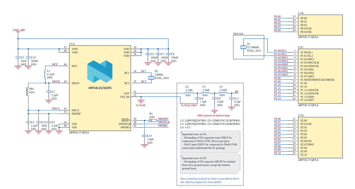
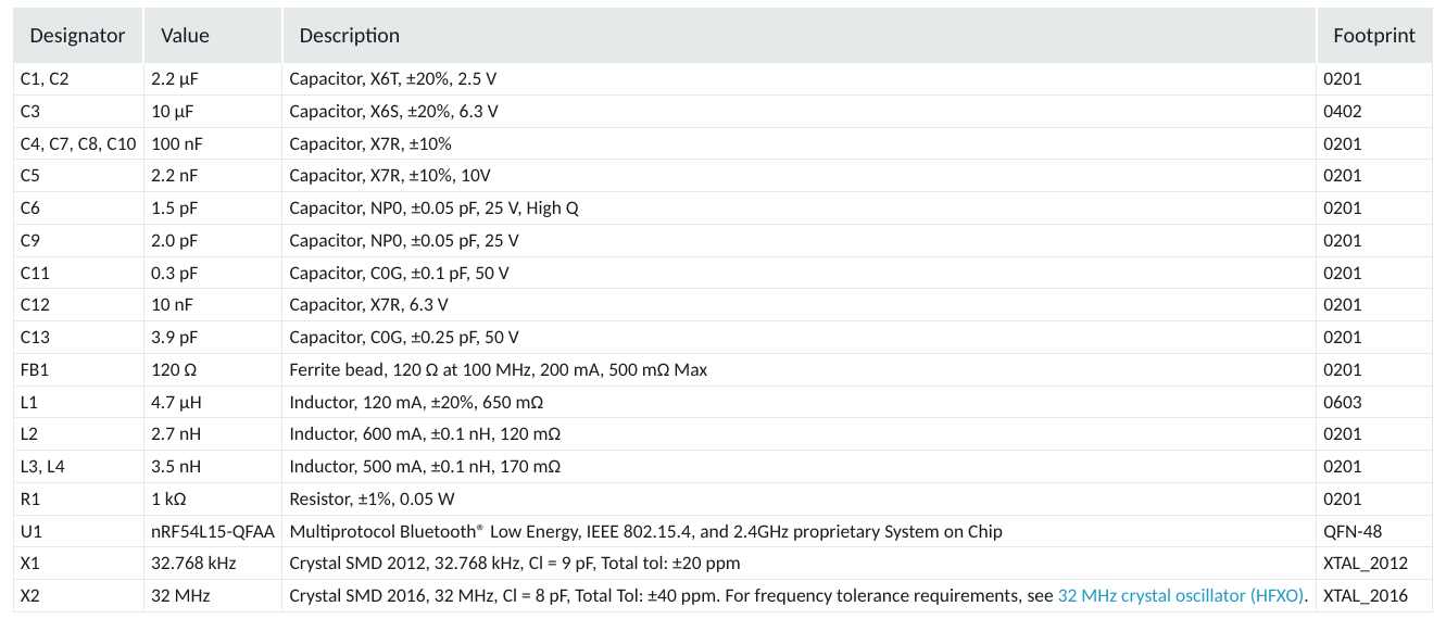
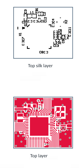
For each Wireless SoC in the nRF54L Series, Nordic Semiconductor provides reference circuitry for each production package (QFN48, CSP98, etc.). Use the PCB layouts and component values from these reference designs to ensure optimal RF performance. Below are the Nordic reference designs for the nRF54L15 SoC, QFN48 package.
Important
Always consult the Datasheet → Hardware and layout → Reference circuitry for the recommended component values and layout for the RF part of your PCB design.
PCB quality also plays a role in power consumption. A poorly manufactured PCB can have low-impedance paths between power and ground caused by solder flux residue, contamination, or poor etching quality. These defects create leakage currents that continuously drain the battery, even when the device is in sleep mode. This is especially problematic for low-power designs where sleep current is measured in microamps, a few microamps of PCB leakage can significantly impact battery life.
In summary, a good RF design maximizes the power that actually leaves the antenna, reducing the need for higher TX power. Combined with a high-quality PCB, this minimizes wasted energy and extends battery life.
5. Power source
Once you understand your device’s estimated power budget (covered in next topics) and its peak current requirements, you can select a battery for your product. At this stage, you also decide whether the design will use a rechargeable battery or a primary (non-rechargeable) cell. By combining these factors, you can then choose the most suitable battery type and determine the required capacity in milliamp-hours (mAh).
Below are common batteries used for Bluetooth LE devices.
Primary (Non-rechargeable) Cells:
Battery Type
Voltage range
Typical Capacity
Notes
CR2032
3.0 V-2.0 V
220-240 mAh
Most common coin cell
CR2025
3.0 V-2.0 V
160-170 mAh
Thinner than CR2032
CR2016
3.0 V-2.0 V
90-100 mAh
Thinnest coin cell
CR2450
3.0 V-2.0 V
600-620 mAh
High capacity coin cell
CR123A
3.0 V-2.0 V
1,400-1,600 mAh
Cylindrical lithium
AA Alkaline
1.5 V-0.9 V
1,500-3,000 mAh
Standard cylindrical
AAA Alkaline
1.5 V-0.9 V
1,000-1,200 mAh
Smaller cylindrical
SR44 (357/303)
1.55 V-1.2 V
150-200 mAh
Silver oxide button cell
SR41 (384/392)
1.55 V-1.2 V
38-45 mAh
Small silver oxide
SR626SW (377)
1.55 V-1.2 V
28-32 mAh
Compact silver oxide
Rechargeable:
Battery Type
Nominal voltage
Typical Capacity
Notes
Li-ion 18650
3.7 V
2,200-3,500 mAh
Common cylindrical cell
Li-ion 14500
3.7 V
600-800 mAh
AA-sized Li-ion
Li-Po (small)
3.7 V
50-500 mAh
Earbuds, small wearables
Li-Po (medium)
3.7 V
500-2,000 mAh
fitness bands, devices with small displays
Li-Po (large)
3.7 V
2,000-5,000 mAh
devices with large displays
AA NiMH
1.2 V
1,900-2,850 mAh
Rechargeable AA
AAA NiMH
1.2 V
800-1,000 mAh
Rechargeable AAA
The recommended voltage for the wireless SoC (1.7 – 3.6 V) for optimal efficiency is covered in the PMIC lesson.
6. Power management IC (PMIC)
A Power Management IC (PMIC) may be necessary when the battery voltage does not directly match the requirements of the components in your design. Common scenarios include:
The battery voltage exceeds the SoC’s maximum input voltage.
The battery voltage falls below the SoC’s minimum operating voltage as it discharges.
Multiple voltage rails are required.
Or if the device requires advanced features such as:
Battery charging (Li-Ion/Li-Po)
Fuel gauging (both for rechargeable battery & primary cells)
Load switches for components
Support for hibernation/ship modes
A PMIC provides regulators, including linear LDO and switching (DCDC) types. A PMIC bridges the gap between your battery and your system’s power requirements. For simple designs with coin cell batteries operating within the SoC’s voltage range, a PMIC may not be necessary. However, for rechargeable batteries, multi-rail systems, or designs requiring advanced power features, a PMIC simplifies the design while improving efficiency, safety, and battery life monitoring.
Prioritize choosing a PMIC with regulators that have low quiescent current and high efficiency across the operating voltage and expected load to minimize power loss.
Switching regulators convert between voltage and current, and power is (mostly) conserved between the input and output. They efficiently accommodate a wide range of supply voltages and can provide either higher (boost) or lower (buck) output voltages relative to the input voltage.
Switching regulator efficiency varies slightly based on load current, input voltage, and output voltage. Typical values are η ≈ 80-95%.
Linear regulators, including LDOs, regulate voltage by acting like a variable resistor that adjusts resistance to maintain a fixed output voltage, with charge mostly conserved between input and output. They are simple and affordable, produce low noise, and have low quiescent current. However, the output voltage must be lower than the input voltage, efficiency is directly limited by the dropout voltage η = V_out/V_in, and excess energy is dissipated as heat proportional to the current due to the voltage drop.
Key comparisons
Parameter
Switching Regulator
LDO
Efficiency
η ≈ 80-95%
η = V_out/V_in
Input Current
I_in = (V_out × I_out)/(V_in × η) + I_q
I_in = I_out + I_q
Quiescent Current
low
very low
Power Loss
Low. Switching + conduction losses
High and depends on the difference between V_in and Vout(V_in – V_out) × I_out.
Example Comparison
Scenario: V_in = 3.7 V (Li-Ion), V_out = 1.8 V, I_out = 10 mA
Switching regulator- Buck (η = 90%):
P_in = 18 mW / 0.90 = 20 mW
P_loss = 2 mW
LDO
η_LDO = 1.8V / 3.7V = 48.6%
P_in = 3.7V × 10 mA = 37 mW
P_out = 1.8V × 10 mA = 18 mW
P_loss = 19mW (wasted as heat!). 17 mW more wasted compared to the buck regulator
When to Use Each
Use Switching regulator when:
Large voltage difference (V_in >> V_out)
Higher load currents (I_out > 1 mA)
Battery life is critical!
Use LDO when:
V_in ≈ V_out (small voltage drop, high efficiency)
Very low I_out (I_q dominates)
Extremely noise-sensitive applications
Nordic provides a comprehensive range of highly efficient PMICs designed for wireless SoCs. See table below:
nPM1100
nPM1300
nPM1304
nPM2100
nPM6001
Battery compatibility
Li-ion, LiPo
Li-ion, LiPo, LiFePO4
Li-ion, LiPo, LiFePO4
AA/AAA, LR44, LiMnO2
–
Battery charger current
20 – 400 mA
32 – 800 mA
4 – 100 mA
–
–
Termination voltage
4.1 – 4.2 V, 4.25 – 4.35 V
3.5 – 4.45 V
3.6 – 4.65 V
–
–
Input voltage
4.1 – 6.7 V
4 – 5.5 V
4 – 5.5 V
0.7 – 3.4 V
3 – 5.5 V
Fuel Gauge
–
Yes
Yes
Yes
–
Regulated power rails
1x Buck
2x Buck + 2x LDO/LS
2x Buck + 2x LDO/LS
1x Boost + 1x LDO/LS
4x Buck + 2x LDO
Max current per Buck
150 mA
200 mA
200 mA
–
550 mA, 200 mA, 2x 150 mA
Max current per Boost
–
–
–
150mA
–
Regulated output voltage
1.8 – 3 V
1 – 3.3 V
1 – 3.3 V
0.8 – 3.3 V
0.5 – 3.3 V
GPIOs, LED drivers
0, 2
5, 3
5, 3
2, 0
3, 0
System management features
Ship mode
WDT, Hibernate Mode, Boot Timer, Power Fail Warning
WDT, Hibernate Mode, Boot Timer, Power Fail Warning
WDT, Hibernate Mode, Boot Timer, Power Fail Warning
WDT, Hibernate Mode
Nordic Developer Academy Privacy Policy
1. Introduction
In this Privacy Policy you will find information on Nordic Semiconductor ASA (“Nordic Semiconductor”) processes your personal data when you use the Nordic Developer Academy.
References to “we” and “us” in this document refers to Nordic Semiconductor.
2. Our processing of personal data when you use the Nordic Developer Academy
2.1 Nordic Developer Academy
Nordic Semiconductor processes personal data in order to provide you with the features and functionality of the Nordic Developer Academy. Creating a user account is optional, but required if you want to track you progress and view your completed courses and obtained certificates. If you choose to create a user account, we will process the following categories of personal data:
Email
Name
Password (encrypted)
Course progression (e.g. which course you have completely or partly completed)
Certificate information, which consists of name of completed course and the validity of the certificate
Course results
During your use of the Nordic Developer Academy, you may also be asked if you want to provide feedback. If you choose to respond to any such surveys, we will also process the personal data in your responses in that survey.
The legal basis for this processing is GDPR article 6 (1) b. The processing is necessary for Nordic Semiconductor to provide the Nordic Developer Academy under the Terms of Service.
2.2 Analytics
If you consent to analytics, Nordic Semiconductor will use Google Analytics to obtain statistics about how the Nordic Developer Academy is used. This includes collecting information on for example what pages are viewed, the duration of the visit, the way in which the pages are maneuvered, what links are clicked, technical information about your equipment. The information is used to learn how Nordic Developer Academy is used and how the user experience can be further developed.
2.2 Newsletter
You can consent to receive newsletters from Nordic from within the Nordic Developer Academy. How your personal data is processed when you sign up for our newsletters is described in the Nordic Semiconductor Privacy Policy.
3. Retention period
We will store your personal data for as long you use the Nordic Developer Academy. If our systems register that you have not used your account for 36 months, your account will be deleted.
4. Additional information
Additional information on how we process personal data can be found in the Nordic Semiconductor Privacy Policy and Cookie Policy.
Nordic Developer Academy Terms of Service
1. Introduction
These terms and conditions (“Terms of Use”) apply to the use of the Nordic Developer Academy, provided by Nordic Semiconductor ASA, org. nr. 966 011 726, a public limited liability company registered in Norway (“Nordic Semiconductor”).
Nordic Developer Academy allows the user to take technical courses related to Nordic Semiconductor products, software and services, and obtain a certificate certifying completion of these courses. By completing the registration process for the Nordic Developer Academy, you are agreeing to be bound by these Terms of Use.
These Terms of Use are applicable as long as you have a user account giving you access to Nordic Developer Academy.
2. Access to and use of Nordic Developer Academy
Upon acceptance of these Terms of Use you are granted a non-exclusive right of access to, and use of Nordic Developer Academy, as it is provided to you at any time. Nordic Semiconductor provides Nordic Developer Academy to you free of charge, subject to the provisions of these Terms of Use and the Nordic Developer Academy Privacy Policy.
To access select features of Nordic Developer Academy, you need to create a user account. You are solely responsible for the security associated with your user account, including always keeping your login details safe.
You will able to receive an electronic certificate from Nordic Developer Academy upon completion of courses. By issuing you such a certificate, Nordic Semiconductor certifies that you have completed the applicable course, but does not provide any further warrants or endorsements for any particular skills or professional qualifications.
Nordic Semiconductor will continuously develop Nordic Developer Academy with new features and functionality, but reserves the right to remove or alter any existing functions without notice.
3. Acceptable use
You undertake that you will use Nordic Developer Academy in accordance with applicable law and regulations, and in accordance with these Terms of Use. You must not modify, adapt, or hack Nordic Developer Academy or modify another website so as to falsely imply that it is associated with Nordic Developer Academy, Nordic Semiconductor, or any other Nordic Semiconductor product, software or service.
You agree not to reproduce, duplicate, copy, sell, resell or in any other way exploit any portion of Nordic Developer Academy, use of Nordic Developer Academy, or access to Nordic Developer Academy without the express written permission by Nordic Semiconductor. You must not upload, post, host, or transmit unsolicited email, SMS, or \”spam\” messages.
You are responsible for ensuring that the information you post and the content you share does not;
contain false, misleading or otherwise erroneous information
infringe someone else’s copyrights or other intellectual property rights
contain sensitive personal data or
contain information that might be received as offensive or insulting.
Such information may be removed without prior notice.
Nordic Semiconductor reserves the right to at any time determine whether a use of Nordic Developer Academy is in violation of its requirements for acceptable use.
Violation of the at any time applicable requirements for acceptable use may result in termination of your account. We will take reasonable steps to notify you and state the reason for termination in such cases.
4. Routines for planned maintenance
Certain types of maintenance may imply a stop or reduction in availability of Nordic Developer Academy. Nordic Semiconductor does not warrant any level of service availability but will provide its best effort to limit the impact of any planned maintenance on the availability of Nordic Developer Academy.
5. Intellectual property rights
Nordic Semiconductor retains all rights to all elements of Nordic Developer Academy. This includes, but is not limited to, the concept, design, trademarks, know-how, trade secrets, copyrights and all other intellectual property rights.
Nordic Semiconductor receives all rights to all content uploaded or created in Nordic Developer Academy. You do not receive any license or usage rights to Nordic Developer Academy beyond what is explicitly stated in this Agreement.
6. Liability and damages
Nothing within these Terms of Use is intended to limit your statutory data privacy rights as a data subject, as described in the Nordic Developer Academy Privacy Policy. You acknowledge that errors might occur from time to time and waive any right to claim for compensation as a result of errors in Nordic Developer Academy. When an error occurs, you shall notify Nordic Semiconductor of the error and provide a description of the error situation.
You agree to indemnify Nordic Semiconductor for any loss, including indirect loss, arising out of or in connection with your use of Nordic Developer Academy or violations of these Terms of Use. Nordic Semiconductor shall not be held liable for, and does not warrant that (i) Nordic Developer Academy will meet your specific requirements, (ii) Nordic Developer Academy will be uninterrupted, timely, secure, or error-free, (iii) the results that may be obtained from the use of Nordic Developer Academy will be accurate or reliable, (iv) the quality of any products, services, information, or other material purchased or obtained by you through Nordic Developer Academy will meet your expectations, or that (v) any errors in Nordic Developer Academy will be corrected.
You accept that this is a service provided to you without any payment and hence you accept that Nordic Semiconductor will not be held responsible, or liable, for any breaches of these Terms of Use or any loss connected to your use of Nordic Developer Academy. Unless otherwise follows from mandatory law, Nordic Semiconductor will not accept any such responsibility or liability.
7. Change of terms
Nordic Semiconductor may update and change the Terms of Use from time to time. Nordic Semiconductor will seek to notify you about significant changes before such changes come into force and give you a possibility to evaluate the effects of proposed changes. Continued use of Nordic Developer Academy after any such changes shall constitute your acceptance of such changes. You can review the current version of the Terms of Use at any time at https://academy.nordicsemi.com/terms-of-service/
8. Transfer of rights
Nordic Semiconductor is entitled to transfer its rights and obligation pursuant to these Terms of Use to a third party as part of a merger or acquisition process, or as a result of other organizational changes.
9. Third Party Services
To the extent Nordic Developer Academy facilitates access to services provided by a third party, you agree to comply with the terms governing such third party services. Nordic Semiconductor shall not be held liable for any errors, omissions, inaccuracies, etc. related to such third party services.
10. Dispute resolution
The Terms of Use and any other legally binding agreement between yourself and Nordic Semiconductor shall be subject to Norwegian law and Norwegian courts’ exclusive jurisdiction.
Switch language?
Progress is tracked separately for each language. Switching will continue from your progress in that language or start fresh if you haven't begun.
Your current progress is saved, and you can switch back anytime.
•Support for nRF54LS05 DK (Available through the early access sampling program) •Support for the nRF54LM20B with Axon NPU for Edge AI applications
Bluetooth LE updates
•Quality of Service module is now production-ready. •New experimental features for RF testing (Direct Test Mode) and low-latency packet handling (LE Flushable ACL).
MCUboot & Partition Manager
•Single-Slot DFU and RAM Load mode are both promoted to fully supported •Partition Manager is officially deprecated in favor of Zephyr's devicetree-based partitioning.