Show that what we measure does not always reflect the internal current draw.
Get an idea of how much current (A) different things draw, so we can identify them in the plot.
Identify spikes and artifacts in the plots, and assess whether or not these are part of the current consumption.
Power modes
From a hardware perspective
The chip can operate in two different power modes: System ON and System OFF.
In System ON, everything inside the chip is functional, and this is also the default power state. This includes the normal sleep state, where the CPU is in idle, and no peripherals are running, which we call “System ON IDLE”.
In System OFF, which is the lowest power state, not much inside the chip is running. It can only wake up on an external signal or GRTC timeout (nRF54 Series only). When it wakes up it goes through a reset, meaning that everything is initialized from the start, like if we did a power on reset.
From a software perspective
A common misunderstanding is that System ON IDLE is a sleep “mode”, a mode you have to actively enter in order to save current between active states; but this is not really the case. From a low level software perspective, there is no such thing as “low power mode” or “sleep mode”. The CPU is either running, or it is waiting for an interrupt. A peripheral is either enabled/active, or it is switched off, consuming no current.
From a hardware perspective the CPU needs to be halted using a WFI (Wait for interrupt) or WFE (Wait for event) call, in order to enter the System ON IDLE state. But this is taken care of automatically in RTOSes like Zephyr.
In Zephyr, System ON IDLE (a.k.a. idle thread) is the default state after booting the chip. What this means is that everything is functional (System ON), and the CPU is in idle, waiting for an interrupt. It is not a mode you can choose to enter. It is the default mode when all threads are finished/paused. (Of course you can claim that calling functions like k_sleep() is a way to “enter System ON IDLE” but basically this just pauses the current thread, defaulting back to the idle thread). More on this can be found in the nRF Connect SDK Intermediate course – Lesson 1 – Scheduler in-depth
What is important in this context is that you use the built-in scheduling (work, timer, etc) functions in Zephyr, for calling your threads. As opposed to creating a blocking for-loop which spins the CPU forever, blocking it from going back to the idle thread, and idling the CPU.
System OFF on the other hand is a sleep mode you have to actively enter. It comes at the cost of resetting the chip on wakeup, which will consume some energy. After a reset, the firmware will reboot, as if we did a power on reset. It will start to reconfigure all registers and reinitialize all the firmware components, which will consume energy. How much energy depends on the firmware.
Internal regulator
Is what we measure always reflecting the actual current consumption inside the chip?
The nRF54 is powered through VDD which supports a given voltage range. Most of the internal circuitry works at a lower voltage, 0.7V to 0.9V. Because of this there is an internal DCDC regulator that steps down the voltage. So what we are measuring is the input current to the internal DCDC regulator, plus leakage on VDD. This means that the power profile does not always reflect the actual current consumption inside the chip, as there is some filtering due to the regulator stage.
An integrated DC/DC converter lets an MCU run efficiently across varying supply conditions while minimizing power loss. The CPU core benefits from low voltage, because power consumption roughly scales with voltage. Lower voltage means much lower energy use. However, when interfacing external components (e.g. 3.3V sensors), we would need a higher voltage, that is why GPIOs are powered from VDD, so that the nRF54 can communicate with other external components using the selected VDD voltage (1.8V to 3.6V) in our design, while the internal circuitry runs at a lower voltage to minimize power loss.
Internal regulators on the nRF54L15 | nRF54L10 | nRF54L05 SoCs
Refresh mode
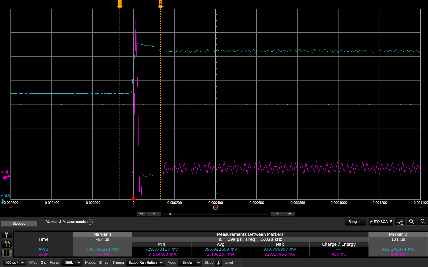
The internal regulator itself also consumes current, what we call quiescent current. In order to save current in low current consumption scenarios, the regulator is not always running. So what happens is that the regulator turns on only for a short time, just enough to charge the output capacitor (DECD capacitor) up to a certain voltage level. Then the internal circuitry is drawing energy from the decoupling capacitor, the voltage over the capacitor drops, and when the voltage reaches a lower threshold the regulator turn on again to recharge the capacitor. This happens over and over again, at a regular interval. The higher the internal current draw, the shorter the interval, because the output capacitor is discharged more rapidly.
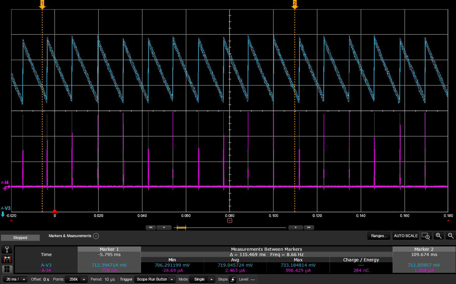
From the measurement equipment perspective, this will look like a series of current bursts into VDD, at a regular interval. But what actually happens is that we have a steady low current consumed inside the chip. This can often be misinterpreted as a periodic “CPU wakeup” or similar, but is in fact just the regulator in refresh mode.
In the plot above you can see the measured VDD current (pink line) being drawn in bursts. This correlates with the internal regulator output voltage (blue line), which can be observed on the DECD pin.
Leakage on VDD versus internal current draw
As explained above, when the internal current draw increases, the frequency of the inrush spikes will increase, and the floor current in between the spikes will stay at the same level. If we are trying to debug a high current consumption issue, we can use this information to verify if the current is actually consumed inside the chip, or if we have a leakage on the VDD domain. If the floor current between the refresh spikes is more than 1 uA, we have leakage on the VDD domain.
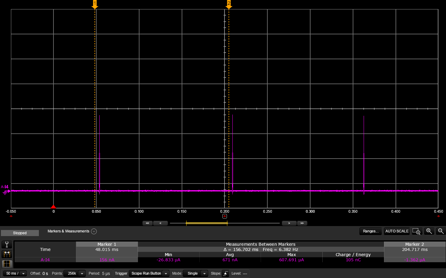
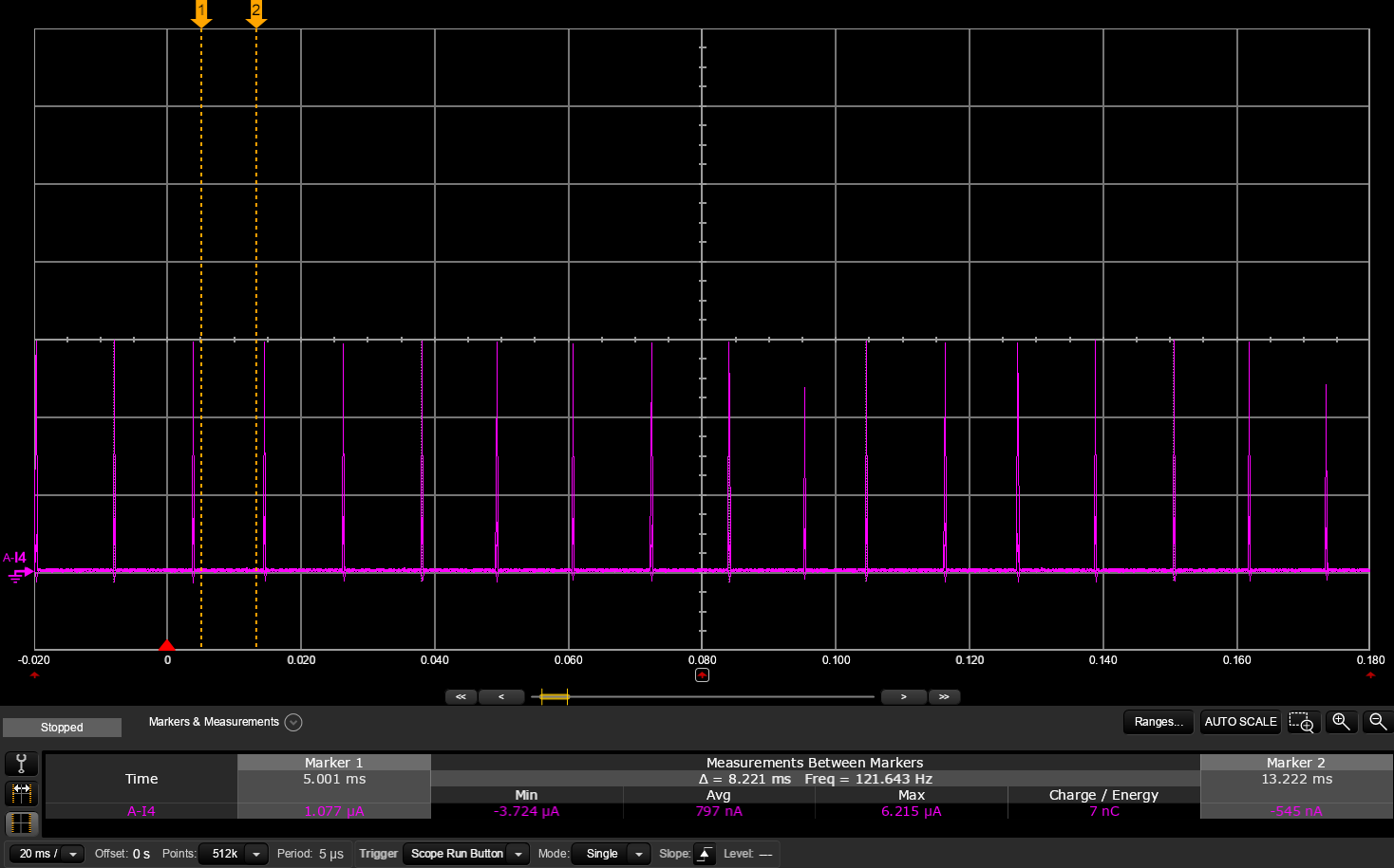
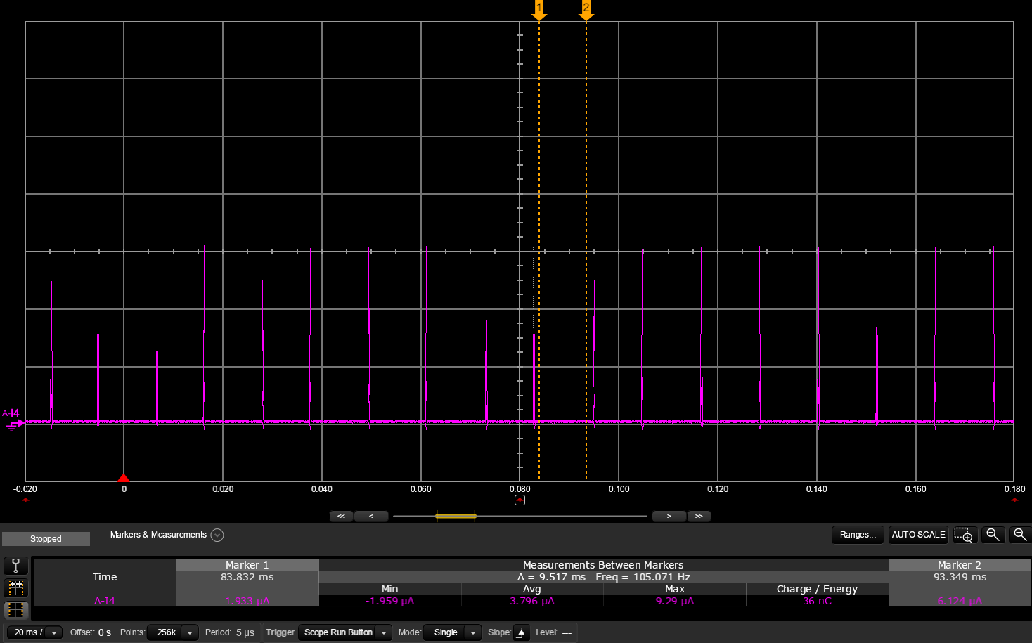
In the table below there are three plots representing different scenarios. Comparing the System OFF case with the System ON IDLE you can see that the spike frequency increases as a result of increased internal current draw. On the DK there are pull-down resistors connected to each of the GPIOs controlling an LED. By setting one of these GPIOs to a high output, we can observe current leakage on the VDD domain going through this pull-down resistor. Comparing the System ON IDLE, with and without LED shows that the floor current increases as a result of increased leakage on one of the GPIOs (which is connected directly to the VDD domain, internally), and that the refresh spike period remains the same, since the internal current draw has not increased.
System OFF
System ON IDLE
System ON IDLE with LED
Plot
Floor current
0.6 µA
0.8 µA
3.8 µA
Spike period
156 ms
11 ms
11 ms
Average current
0.7 µA
2.4 µA
5.5 µA
This information can be valuable when debugging current consumption issues as you can separate the VDD current draw and the internal current draw by looking at the spike frequency versus the floor current. This will only work in idle mode, as the spike period is long enough to be observed by the measurement equipment.
In our example above with “System ON IDLE” versus “System ON IDLE with LED,” we see that the expected floor current is 0.8uA, but 3.8uA is measured when the LED is lit. This means we have 3.0uA too much. In the measurement above the supply voltage is 3.0V. Therefore, these 3.0uA could be caused by a resistor with a value of R = U/I = 3V / 3.0uA = 1MOhm. If we take a look at the DK’s schematic, we’ll find what we’re looking for:
Resistive load on VDD
Another way of separating internal current consumption and VDD consumption in our measurements is taking into consideration that the internal current draw is scaled through the DC/DC regulator. What this means is that when decreasing the input voltage on VDD, we would get a higher current consumption if current is consumed inside the chip, but we would get a lower current consumption if the current was caused by a resistive load on VDD.
A resistive load on VDD will just follow Ohm’s law; a higher voltage means a higher current. As opposed to the load inside the chip; a higher voltage means a lower current, as the energy is close to preserved through the DC/DC regulator. More information in this section: Current measurement fundamentals | Power and energy
We can use this information when debugging current consumption issues. Try to increase or decrease the voltage and observe if the current goes up or down.
Regulator output voltage
The internal circuitry operates at different voltages depending on the current draw. During idle the regulator output voltage is 0.7V, and as soon as it wakes up the voltage is 0.9V. This will lead to an inrush current into the DEC capacitors. Most of this energy is regained when the chip goes back to sleep, as it will draw current only from the DEC capacitors until it reaches the 0.7V idle voltage again
Wake up from idle
Back to idle
DECD voltage increase from 0.7V to 0.9V The inrush current peak value will depend the series resistance on VDD, but the charge/energy will be the same.
Voltage over the DECD capacitor decreases back to 0.7V as energy is drawn from the capacitor, until the lower limit at 0.7V, when the refresh mode starts up again
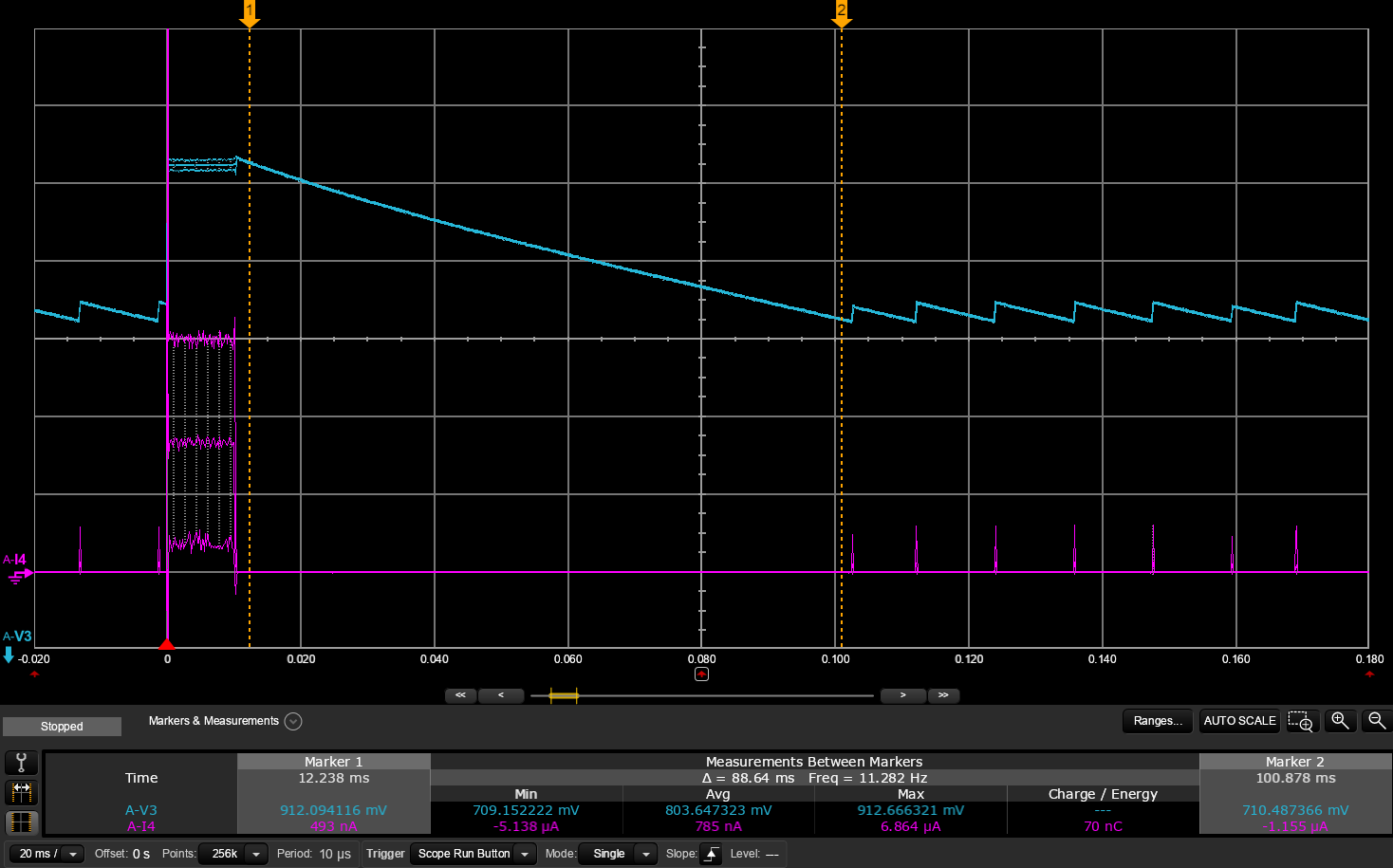
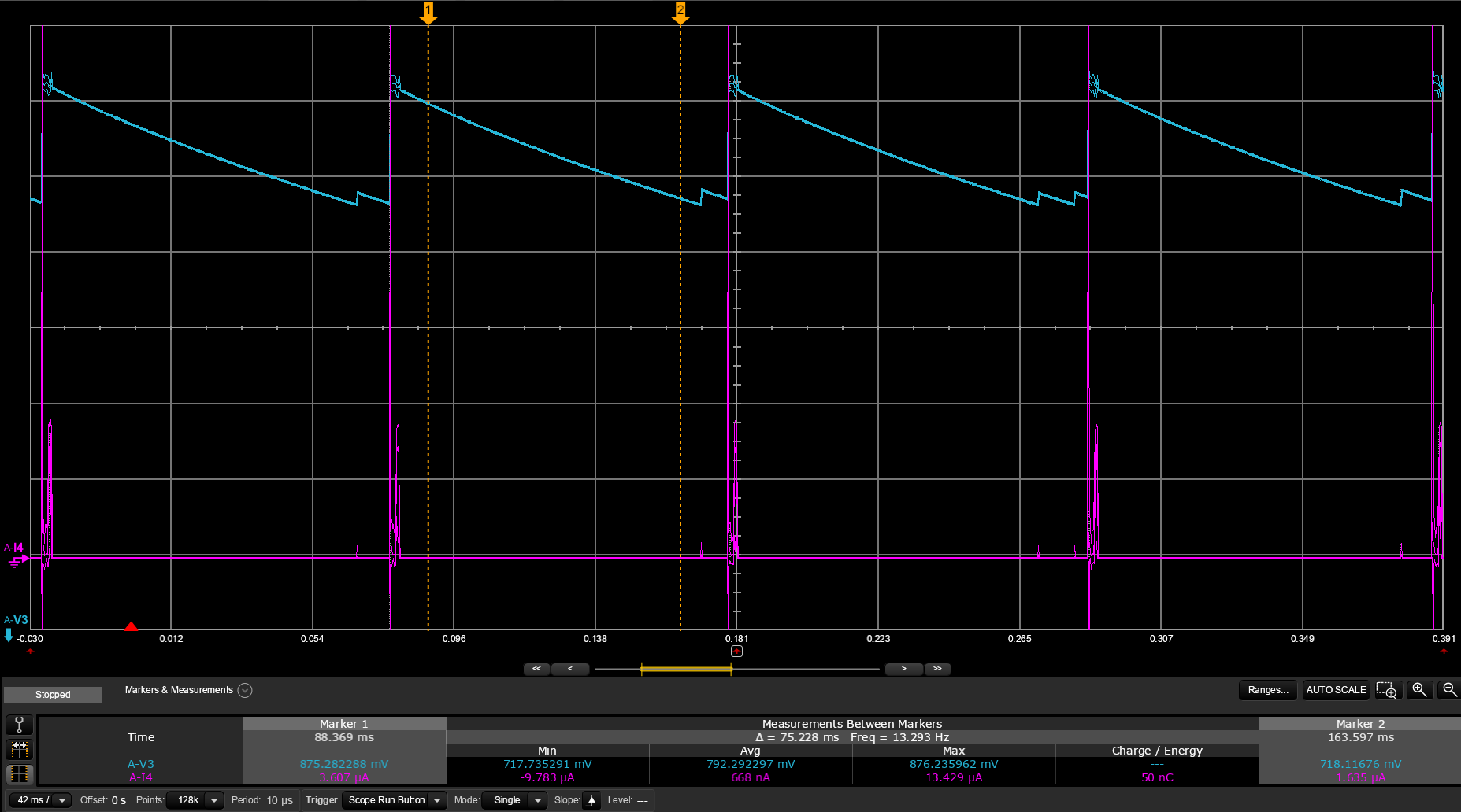
An important aspect here is that when having wakeup intervals shorter that around 100 ms, it will always draw current from the DEC capacitors during idle. It will not have time to go into refresh mode before the next wakeup. This means that the measured idle current between the events will be much lower than the actual idle current, and may be misleading. As a consequence, if you want to verify the idle current in your project, it is important that the idle period is significantly longer than this, and you should not include the first 100ms in your measurements. You could temporarily adjust the advertising interval, or connection interval, to around 1 second, for the purpose of finding the correct idle current.
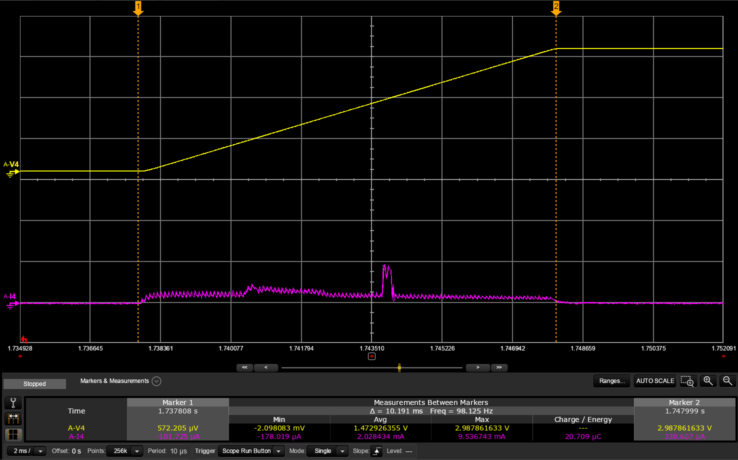
Here is an example of Bluetooth LE advertising occurring every 100 ms. The measured average current in between the advertising events is 668 nA. This does not reflect the actual idle current, as it should be closer to 3 uA (on this specific chip, nRF54L15)
Inrush current when turning on power supply
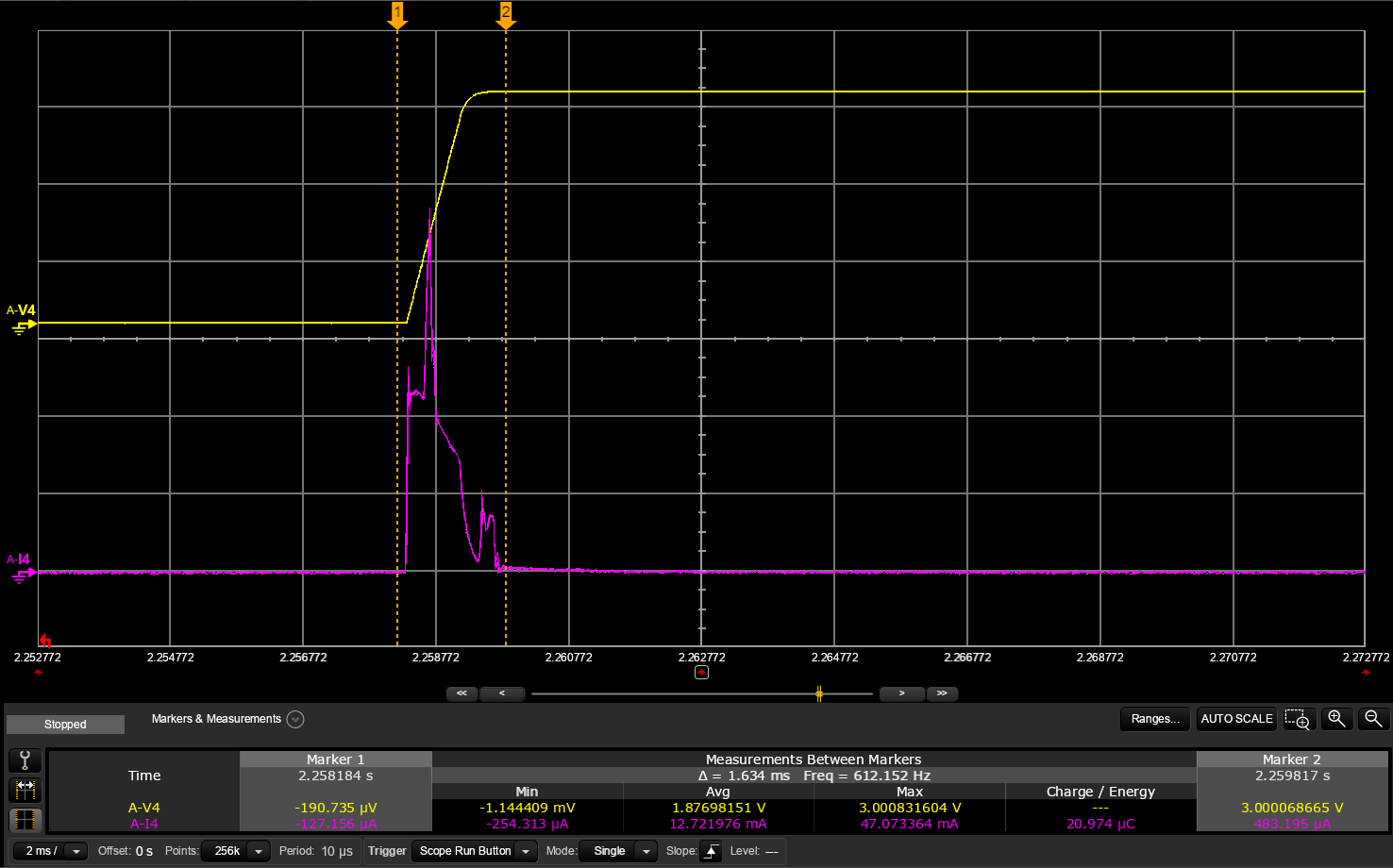
When ramping up the VDD voltage from 0V to the operating voltage, there will flow quite a lot of current into the decoupling capacitors on VDD, as well as DECD and DECA.
In the plot below we first have a slow VDD ramp from 0 to 3V of around 10 ms, this gives us a peak current of about 9.5 mA. If the ramp up is faster, i.e. internal resistance of the supply is lower, the peak current might get significantly higer. In the example below the peak current is 47 mA over a 1 ms ramp. Note that the total charge is the same in both plots. Because the same amount of charge is needed to charge up the capacitors, regardless of the ramp time.
Fast ramp up
Slow ramp up
1 ms ramp up Peak current: 47 mA Total charge: 21 uC
10 ms ramp up Peak current: 9.5 mA Total charge: 21 uC
The peak current observed when ramping up the VDD supply is often misinterpreted as the MCU boot current, CPU boot code, or similar. However, this is an inevitable consequence of having a capacitive load, like decoupling capacitors and similar on the circuit board.
Floating input GPIO
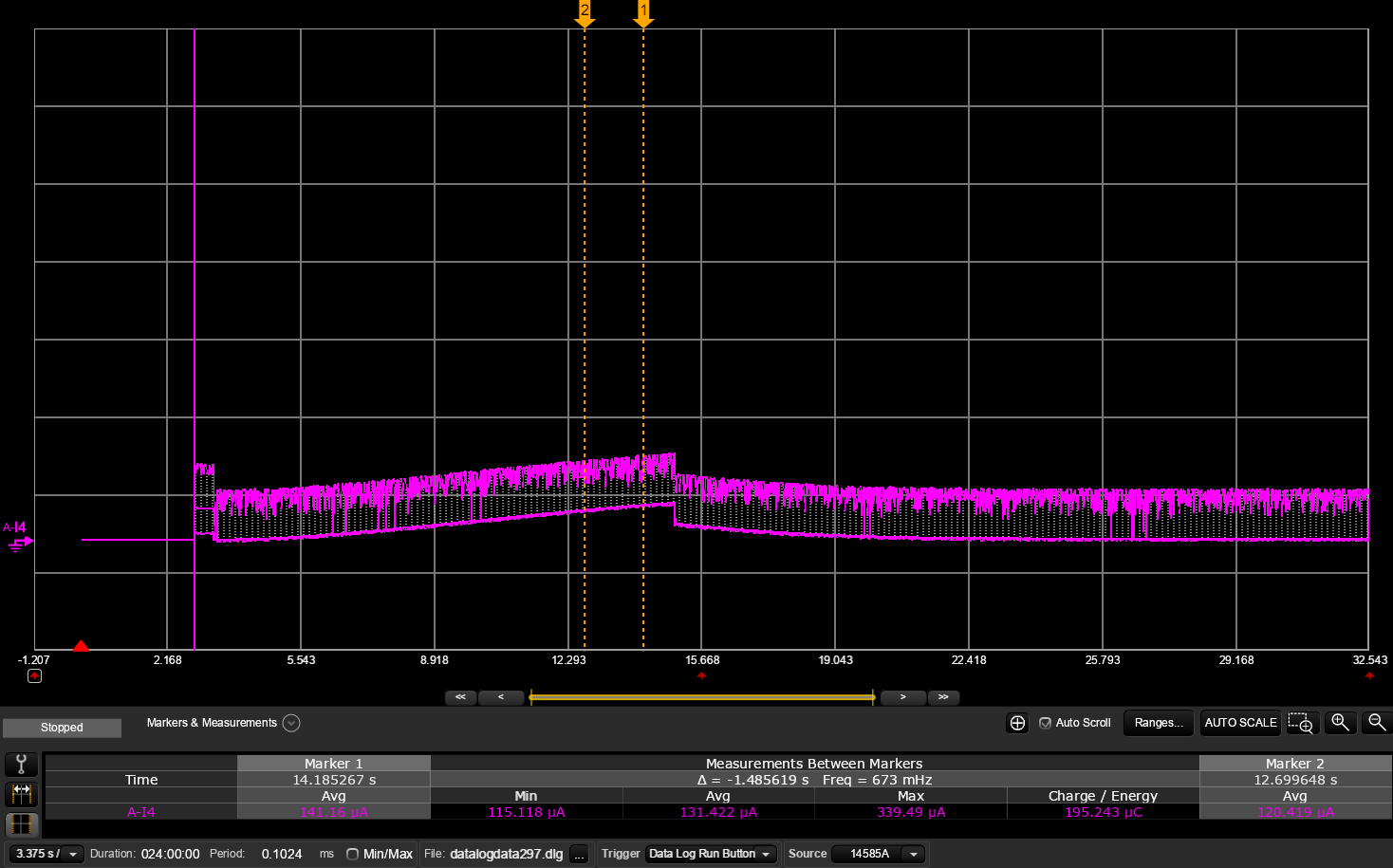
The default configuration for a GPIO after boot is what we call “disconnected input”. Meaning that the pin is configured as an input, and that the input buffer responsible for sensing the level is disconnected. In this mode it can not source or sink any current. If you want to use the GPIO as an input from an external sensor or similar, you need to set the input buffer as “connected”. In this mode there will be no additional current draw if the voltage is at the defined logic 1 or 0 voltage levels. However, if the voltage is residing somewhere in between these values, there will flow a current through the input buffer. The amount of current depends on the voltage. So if you happen to configure a GPIO as a connected input, and it is not driven externally, i.e. floating, you will get a undeterministic current draw on the VDD domain. So, a floating input node might be difficult to debug, unless you know this is an issue, because the current consumption will be pretty random. And it will change all the time.
Here is a plot showing P0.04 configured as a floating input node. The first spike is the power on reset, then current starts to drift upwards, and then back down again. The current reaches almost 150uA, while it should be at a stable 3uA
Which peripherals will consume current, and how much?
In order to debug current consumption issues, we should have an idea of what different components inside the chip consumes. There is a very large difference between idle current and active currents.
A common misunderstanding is that if the current consumption is high, the chip is not going into “sleep mode”, or there is a missing “sleep mode” config.
As we discussed earlier, the CPU will always go into idle when all threads have finished. So what we should be looking into is to try and correlate the excessive current consumption with a peripheral’s run current. But in order to do that we need some ballpark numbers on what we can expect.
We can divide current consumption into categories.
Current consumption
Notes
Base leakage
System OFF
< 1 uA
Base leakage current, which will always be present
System ON base current
< 1 uA
SRAM leakage
10-20 nA per 32k block
Unused blocks can be turned off to save current
32k clock
LFXO or LFRC
0.1-0.7 uA
GRTC
~ 0.1 uA
At this stage we have reached normal operating condition for an application, and is what we call System ON IDLE
< 3 uA
Sum of the above= System ON IDLE
Power domains
Peripherals waiting for PIN interrupt
10-50 uA
SPIS/TWIS
GPIOTE IN event
10-50 uA
High frequency clock
HFXO run current
100-200 uA
If better HF accuracy is needed, i.e. radio
Serial peripheral run current
0.2 mA – 1 mA
SPI, TWI, UART
TIMER
0.2 mA – 1 mA
LFRC calibration
2-3 mA for a few ms
CPU
2-5 mA
Depends on the task, wait states, etc
Radio
2 – 20 mA
depending on TX output power
In Lesson 5, Exercise 2, we will examine this further by measuring the impact of enabling various peripherals such as UART, watchdog, timers from different power domains, and PWM outputs, including both standard and low power GRTC, on average current and System ON IDLE current.
Device to device and temperature variation
Due to the process technology there will always be device to device variations when it comes to current consumption. Some devices are what we call “fast” devices, and others are “slow” devices. From a timing perspective all samples are tested to be within certain test limits, so on a functional basis, they behave the same. But in terms of current consumption there will be a difference. Fast devices will consume more current.
Also when it comes to temperature variations, devices will become “faster” at higher temperatures, which means that the current consumption will increase.
The biggest variation will be in what we call the leakage current, not in the active current. So leakage current is the current that is leaking inside the transistors when they are turned on, but still in idle. Meaning that the base leakage, i.e. System ON all IDLE, and SRAM leakage will have the biggest variation. The more SRAM blocks that are powered on, the bigger the variation across devices and temperature, in idle.
In the datasheet, only the typical value is listed for System ON IDLE with full RAM retention. But in reality the typical value represents the mean value over a normal distribution.
This is important to be aware of when trying to match the datasheet numbers for the idle current with your measurements. You might not get the exact same value.
Now the problem is, how do we know that the deviation from the datasheet number is caused by device to device variation or a measurement issue?
As mentioned above, it is the idle leakage including the SRAM that leads to most of the variation. So verifying our test setup with a firmware where this variation is minimized would be the best approach. In other words, verifying your test setup with a System OFF sample without SRAM retention, is the way to go. The System OFF sample will consume less than 1 uA, so if your measuring tools also shows less than 1 uA, or ideally the same as the datasheet number, you know that your measurement setup is good, and that there is no external leakage.
This leads us on to the next section on how to further verify our test setup, and debugging current consumption issues
Verifying the measurement setup
Measure on a firmware with a known current consumption
When compiling a sample in nRF Connect SDK, the samples have UART logging enabled by default. Most samples are also using LEDs for different types of feedback, and they have full SRAM retention enabled.
If we start by measuring directly on one of these samples, we often do not know what to expect, and it is difficult to know if what we measure is correct. Therefore it is very important that we always verify our setup before we start.
We can verify our setup with the System OFF sample. Later in this course we will use pre-compiled hex-files which do have a known current consumption. And also explain how we can create our own System OFF firmware. All of this in Exercise 1.
Why is the System OFF sample a good starting sample?
It is possible to turn off all SRAM, which minimizes device to device variation. In System ON IDLE, this is more difficult as the RAM is needed for the firmware, and it will crash if all RAM is switched off.
We know that no peripherals or power domains are active
Should match the datasheet pretty close. Or at least if you end up at sub 1uA then the offset will probably be negligible for other measurements
If we now get a higher current than what is specified in the datasheet, there are four possible reasons:
Our measurement equipment is not showing the correct current
Could be that the accuracy is not good enough.
Range is fixed, and set to a higher current consumption range, not able to measure the sub 1 uA range.
Try with a simple handheld multimeter or a different instrument, and see if you read the same current.
The chip is not in System OFF
We can verify this by looking at the refresh spike period. It should be around 100 to 200 ms. Look at the section above for more info
We have leakage on the VDD domain
Can be leakage due to other components being powered from the same VDD
As explained above, if the System OFF sample gives us a higher current than the datasheet number, this can be due to leakage on the VDD domain. Leakage current in this context means current flowing into the VDD domain that is not consumed by the DUT itself. This can be external components powered by the same VDD, but also powered through GPIOs on the nRF54, since the GPIOs are powered directly from the VDD domain.
On the DK we can use the board controller to physically disconnect all GPIOs, and the current measurement header will only reflect what is actually consumed by the DUT.
On custom boards it can be a bit more tricky, but it depends on the design, and how well components are isolated for current measurements. You need to look at the schematic and identify all possible paths where current can flow.
Examples of VDD leakage current
Example schematic
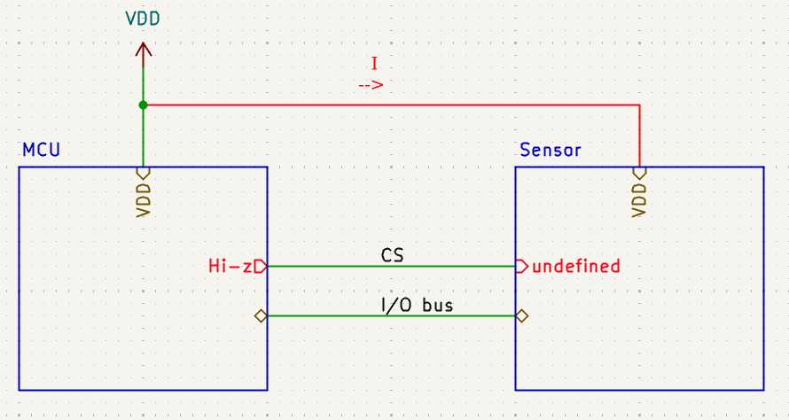
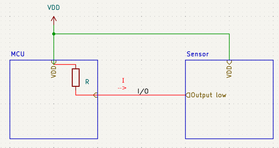
Chip select pins or similar configured as high-z ->Current will flow into VDD on the external component as it is not in a defined state ->Make sure that outputs that must be in a defined state, like chip select pins, are always defined
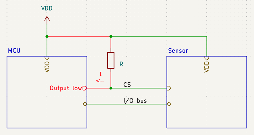
External pull-up, but actively driven low ->Current will flow from VDD through pull-up, into the MCU GPIO ->Make sure that pin is left in a high impedance state, when in idle
Internal pull-up, but driven low externally ->Current will flow from MCU through it’s internal pull-up, out to the external component ->Make sure that no pull resistors are configured if input GPIO is actively driven externally
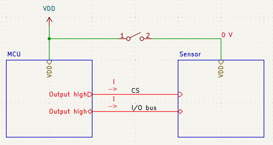
Powering external components ->If an external component is not powered but connected through GPIOs, it will be back powered through the GPIOs if they are driven high. ->Always set GPIOs to un-powered components to the “disconnected input” state
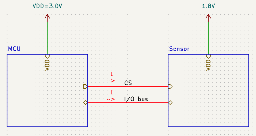
External components at different voltage level ->Current will flow through GPIOs if VDD voltages do not match ->Use a level converter
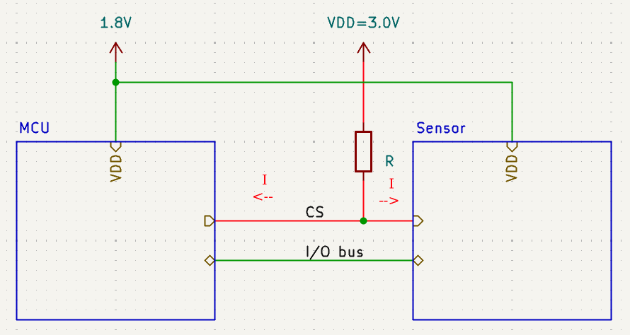
Pull-up to a different voltage level ->Current will flow from the highest voltage and back-power the MCU ->Make sure that all pull-up resistors are connected to the same VDD net as the MCU/sensor
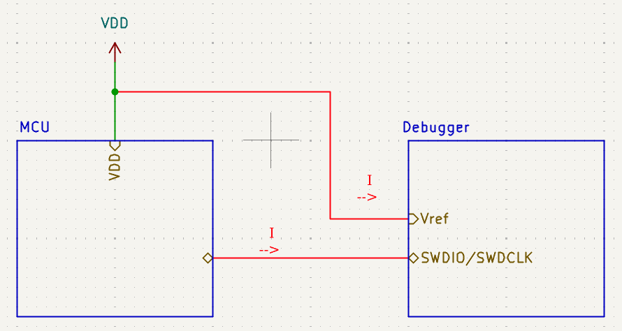
SWD leakage ->Current might flow out of the SWD interface into the debugger, and also from VDD to the voltage sensing circuit in the debugger ->Always disconnect debugger when doing measurements **–>On the DK the debugger can be disconnected through the board controller (Board Configurator app in nRF Connect for Desktop)
Final words on debugging current consumption issues
Common pitfall when debugging current consumption issues is to start by commenting out sections of the code, or disabling things in the devicetree, to see if current decreases, in order to find the culprit. Let’s say we try this approach but instead we observe that the current consumption increases or stays approximately the same. Our conclusion would be that the removed piece is not responsible for our high current consumption. But what actually happened is that this piece in fact was responsible for the high current consumption, but removing it made another issue appear. It could be as simple as a hardfault. (So, always check if the code is actually running after making changes), but it could also be other things, like removing a section in devicetree leading to incorrectly configured GPIOs. E.g. a CS pin to an external SPI sensor, which is left floating.
The best approach for debugging current measurement issues is actually going the opposite way. Starting out with for example the blinky sample, making sure that you have a normal idle current first. Then you continue by adding piece by piece from your main project, measuring current for each iteration.
This may sound like a lot of work, especially if you have a large project you need to power optimize, but in the end it will probably save you time.
This also means that measuring current as an active part of firmware development, is a good approach. Starting with current measurements as the first thing you do when starting a new project, making sure that the idle current is low, and that every iteration and code change after that, do not give you an elevated idle current, or similar.
Starting with power optimizations after the firmware development is finished is not a good idea, and may lead to a lot of additional work, and last minute design changes. Both hardware and software changes.
Another advantage with current measurements during firmware development is that it is a great debugging tool. Looking at the power profile can give you detailed information about what the firmware is doing, or not doing. Especially if you combine it with GPIO toggling, and are able to plot both current consumption and GPIOs in the same plot (The PPK can do this).
Nordic Developer Academy Privacy Policy
1. Introduction
In this Privacy Policy you will find information on Nordic Semiconductor ASA (“Nordic Semiconductor”) processes your personal data when you use the Nordic Developer Academy.
References to “we” and “us” in this document refers to Nordic Semiconductor.
2. Our processing of personal data when you use the Nordic Developer Academy
2.1 Nordic Developer Academy
Nordic Semiconductor processes personal data in order to provide you with the features and functionality of the Nordic Developer Academy. Creating a user account is optional, but required if you want to track you progress and view your completed courses and obtained certificates. If you choose to create a user account, we will process the following categories of personal data:
Email
Name
Password (encrypted)
Course progression (e.g. which course you have completely or partly completed)
Certificate information, which consists of name of completed course and the validity of the certificate
Course results
During your use of the Nordic Developer Academy, you may also be asked if you want to provide feedback. If you choose to respond to any such surveys, we will also process the personal data in your responses in that survey.
The legal basis for this processing is GDPR article 6 (1) b. The processing is necessary for Nordic Semiconductor to provide the Nordic Developer Academy under the Terms of Service.
2.2 Analytics
If you consent to analytics, Nordic Semiconductor will use Google Analytics to obtain statistics about how the Nordic Developer Academy is used. This includes collecting information on for example what pages are viewed, the duration of the visit, the way in which the pages are maneuvered, what links are clicked, technical information about your equipment. The information is used to learn how Nordic Developer Academy is used and how the user experience can be further developed.
2.2 Newsletter
You can consent to receive newsletters from Nordic from within the Nordic Developer Academy. How your personal data is processed when you sign up for our newsletters is described in the Nordic Semiconductor Privacy Policy.
3. Retention period
We will store your personal data for as long you use the Nordic Developer Academy. If our systems register that you have not used your account for 36 months, your account will be deleted.
4. Additional information
Additional information on how we process personal data can be found in the Nordic Semiconductor Privacy Policy and Cookie Policy.
Nordic Developer Academy Terms of Service
1. Introduction
These terms and conditions (“Terms of Use”) apply to the use of the Nordic Developer Academy, provided by Nordic Semiconductor ASA, org. nr. 966 011 726, a public limited liability company registered in Norway (“Nordic Semiconductor”).
Nordic Developer Academy allows the user to take technical courses related to Nordic Semiconductor products, software and services, and obtain a certificate certifying completion of these courses. By completing the registration process for the Nordic Developer Academy, you are agreeing to be bound by these Terms of Use.
These Terms of Use are applicable as long as you have a user account giving you access to Nordic Developer Academy.
2. Access to and use of Nordic Developer Academy
Upon acceptance of these Terms of Use you are granted a non-exclusive right of access to, and use of Nordic Developer Academy, as it is provided to you at any time. Nordic Semiconductor provides Nordic Developer Academy to you free of charge, subject to the provisions of these Terms of Use and the Nordic Developer Academy Privacy Policy.
To access select features of Nordic Developer Academy, you need to create a user account. You are solely responsible for the security associated with your user account, including always keeping your login details safe.
You will able to receive an electronic certificate from Nordic Developer Academy upon completion of courses. By issuing you such a certificate, Nordic Semiconductor certifies that you have completed the applicable course, but does not provide any further warrants or endorsements for any particular skills or professional qualifications.
Nordic Semiconductor will continuously develop Nordic Developer Academy with new features and functionality, but reserves the right to remove or alter any existing functions without notice.
3. Acceptable use
You undertake that you will use Nordic Developer Academy in accordance with applicable law and regulations, and in accordance with these Terms of Use. You must not modify, adapt, or hack Nordic Developer Academy or modify another website so as to falsely imply that it is associated with Nordic Developer Academy, Nordic Semiconductor, or any other Nordic Semiconductor product, software or service.
You agree not to reproduce, duplicate, copy, sell, resell or in any other way exploit any portion of Nordic Developer Academy, use of Nordic Developer Academy, or access to Nordic Developer Academy without the express written permission by Nordic Semiconductor. You must not upload, post, host, or transmit unsolicited email, SMS, or \”spam\” messages.
You are responsible for ensuring that the information you post and the content you share does not;
contain false, misleading or otherwise erroneous information
infringe someone else’s copyrights or other intellectual property rights
contain sensitive personal data or
contain information that might be received as offensive or insulting.
Such information may be removed without prior notice.
Nordic Semiconductor reserves the right to at any time determine whether a use of Nordic Developer Academy is in violation of its requirements for acceptable use.
Violation of the at any time applicable requirements for acceptable use may result in termination of your account. We will take reasonable steps to notify you and state the reason for termination in such cases.
4. Routines for planned maintenance
Certain types of maintenance may imply a stop or reduction in availability of Nordic Developer Academy. Nordic Semiconductor does not warrant any level of service availability but will provide its best effort to limit the impact of any planned maintenance on the availability of Nordic Developer Academy.
5. Intellectual property rights
Nordic Semiconductor retains all rights to all elements of Nordic Developer Academy. This includes, but is not limited to, the concept, design, trademarks, know-how, trade secrets, copyrights and all other intellectual property rights.
Nordic Semiconductor receives all rights to all content uploaded or created in Nordic Developer Academy. You do not receive any license or usage rights to Nordic Developer Academy beyond what is explicitly stated in this Agreement.
6. Liability and damages
Nothing within these Terms of Use is intended to limit your statutory data privacy rights as a data subject, as described in the Nordic Developer Academy Privacy Policy. You acknowledge that errors might occur from time to time and waive any right to claim for compensation as a result of errors in Nordic Developer Academy. When an error occurs, you shall notify Nordic Semiconductor of the error and provide a description of the error situation.
You agree to indemnify Nordic Semiconductor for any loss, including indirect loss, arising out of or in connection with your use of Nordic Developer Academy or violations of these Terms of Use. Nordic Semiconductor shall not be held liable for, and does not warrant that (i) Nordic Developer Academy will meet your specific requirements, (ii) Nordic Developer Academy will be uninterrupted, timely, secure, or error-free, (iii) the results that may be obtained from the use of Nordic Developer Academy will be accurate or reliable, (iv) the quality of any products, services, information, or other material purchased or obtained by you through Nordic Developer Academy will meet your expectations, or that (v) any errors in Nordic Developer Academy will be corrected.
You accept that this is a service provided to you without any payment and hence you accept that Nordic Semiconductor will not be held responsible, or liable, for any breaches of these Terms of Use or any loss connected to your use of Nordic Developer Academy. Unless otherwise follows from mandatory law, Nordic Semiconductor will not accept any such responsibility or liability.
7. Change of terms
Nordic Semiconductor may update and change the Terms of Use from time to time. Nordic Semiconductor will seek to notify you about significant changes before such changes come into force and give you a possibility to evaluate the effects of proposed changes. Continued use of Nordic Developer Academy after any such changes shall constitute your acceptance of such changes. You can review the current version of the Terms of Use at any time at https://academy.nordicsemi.com/terms-of-service/
8. Transfer of rights
Nordic Semiconductor is entitled to transfer its rights and obligation pursuant to these Terms of Use to a third party as part of a merger or acquisition process, or as a result of other organizational changes.
9. Third Party Services
To the extent Nordic Developer Academy facilitates access to services provided by a third party, you agree to comply with the terms governing such third party services. Nordic Semiconductor shall not be held liable for any errors, omissions, inaccuracies, etc. related to such third party services.
10. Dispute resolution
The Terms of Use and any other legally binding agreement between yourself and Nordic Semiconductor shall be subject to Norwegian law and Norwegian courts’ exclusive jurisdiction.
Switch language?
Progress is tracked separately for each language. Switching will continue from your progress in that language or start fresh if you haven't begun.
Your current progress is saved, and you can switch back anytime.
•This release includes Long-Term Support (LTS) for five years.
•Patch (minor) releases will address security vulnerabilities and critical bug fixes.
•API stability is guaranteed; breaking changes are only introduced when required by a security fix.
•Notifications for critical bug fixes and security updates via the myNordic notification system (mynordic.nordicsemi.com)
General updates
•Support for nRF54LS05 DK (Available through the early access sampling program) •Support for the nRF54LM20B with Axon NPU for Edge AI applications
Bluetooth LE updates
•Quality of Service module is now production-ready. •New experimental features for RF testing (Direct Test Mode) and low-latency packet handling (LE Flushable ACL).
MCUboot & Partition Manager
•Single-Slot DFU and RAM Load mode are both promoted to fully supported •Partition Manager is officially deprecated in favor of Zephyr's devicetree-based partitioning.