The first thing we should do before starting with current measurements is to verify our setup. In this exercise we will use the system OFF mode to check if we have any leakage current in our setup, and check if we are able to achieve the sub 1 uA specified in the datasheet.
To ensure that the firmware we run is actually entering System OFF, we will use pre-compiled hex files.
We will also learn how we can compile our own System OFF firmware.
Exercise steps
1. Measurement setup
1.1 Connect the measuring equipment to the DK.
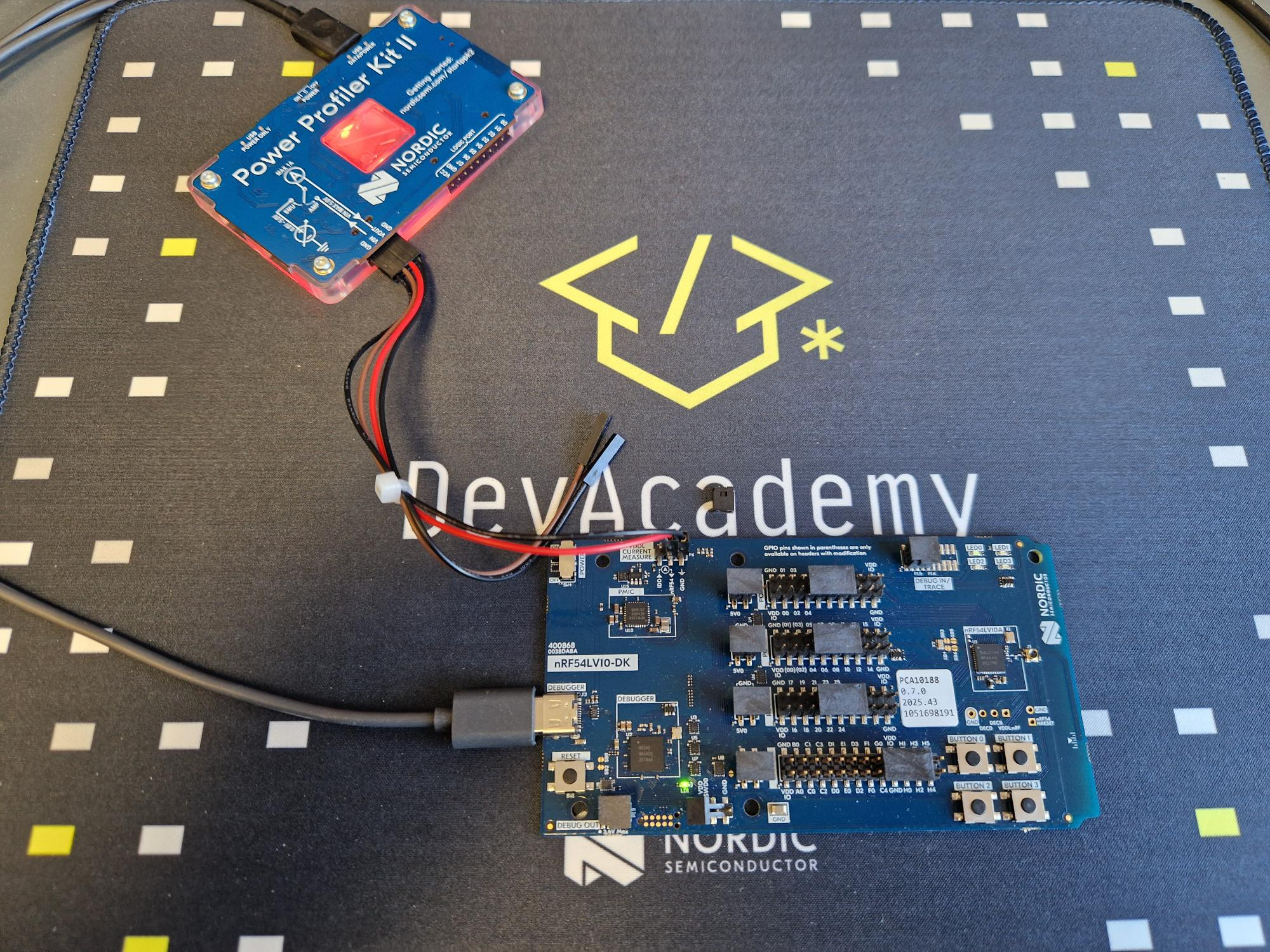
First we want to connect our measuring equipment to the DK, in our case the Power Profiler Kit II (PPK2) in source meter mode. Using source meter mode is always the best option, so if you have equipment that can output voltage and measure current at the same time (SMU), you should go for this option.
It is important that the USB cable to the DK is connected. The DK is not designed to work without the USB cable connected, and you will get leakage current.
Using this setup, we can program new firmware to our device without reconnecting any wires. Just make sure that the SMU power output is turned on, and then you would typically power cycle the device after flashing, using the SMU software.
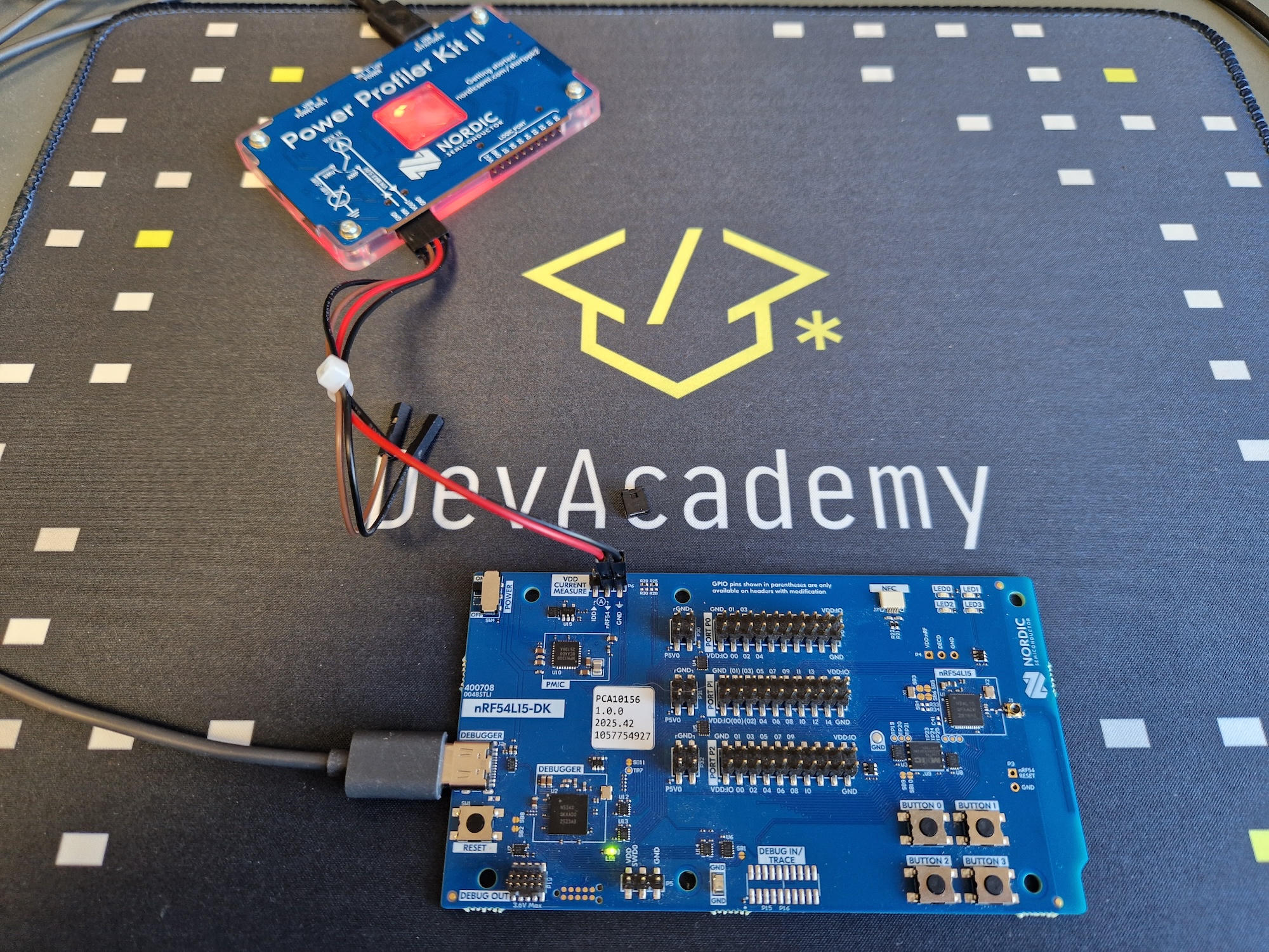
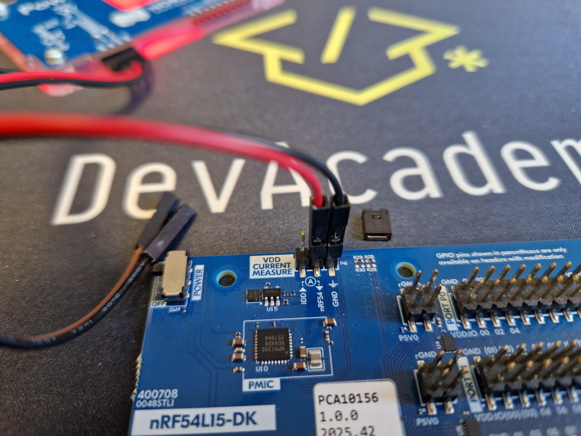
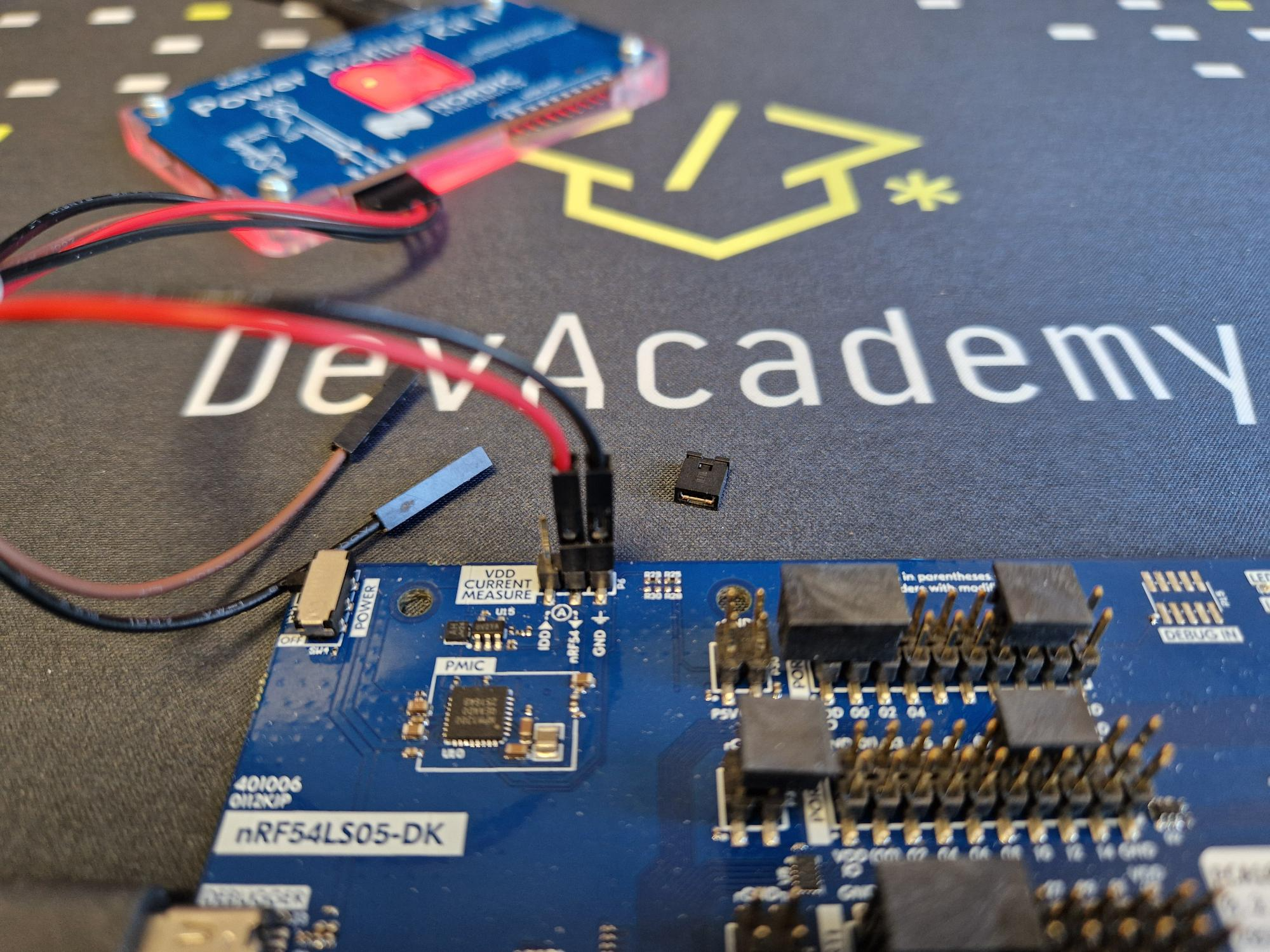
Remove the jumper on P6 (VDD CURRENT MEASURE), connect VOUT on the PPK2 to nRF54 on the P6 header (red cable in the image below) and GND to GND on the P6 header (black cable in the image below)
P6 close up on the nRF54L15 DK
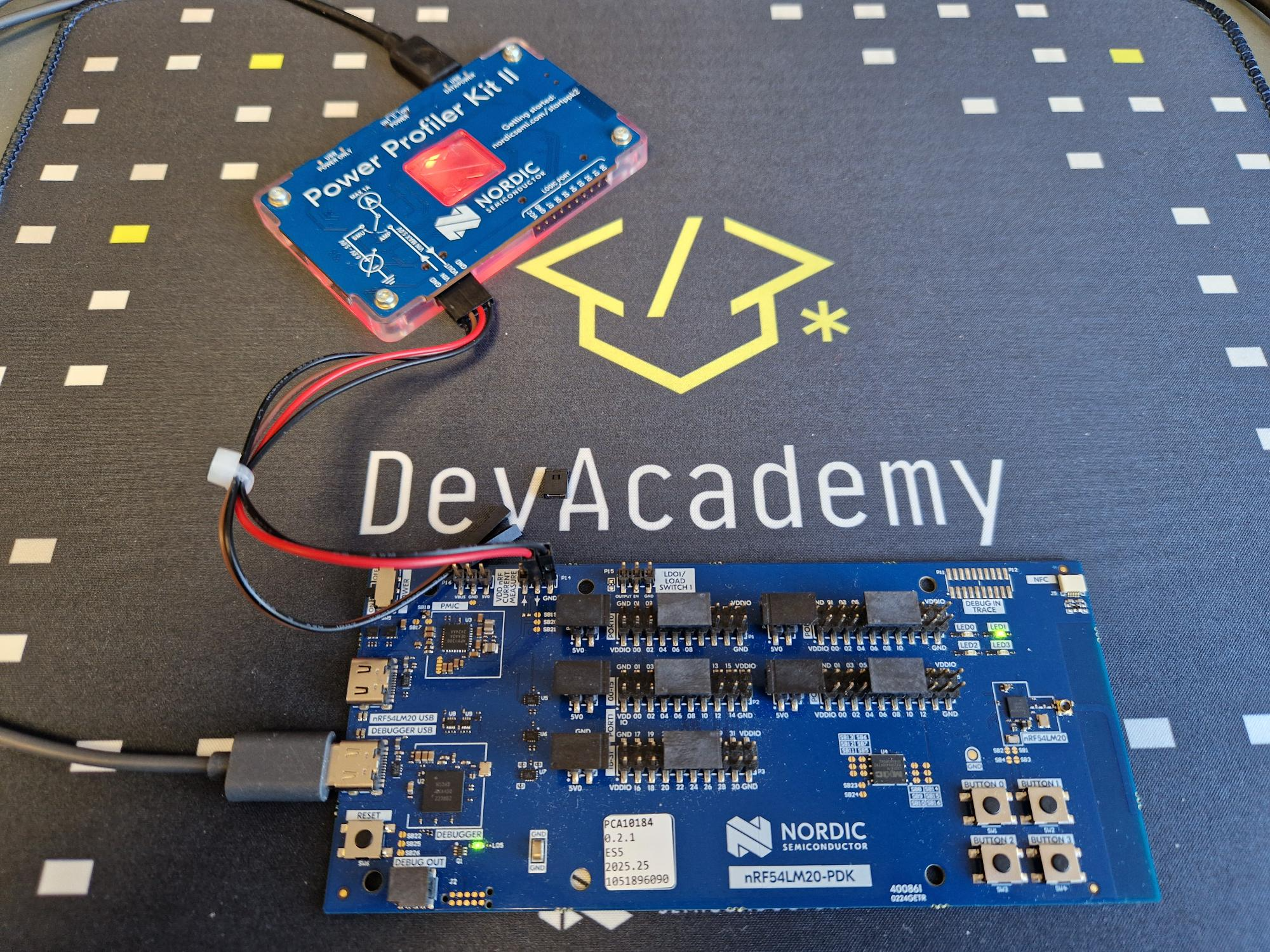
Remove the jumper on P14 (VDD nRF CURRENT MEASURE), connect VOUT on the PPK2 to the middle pin on the P14 header (red cable in the image below) and GND to GND on the P14 header (black cable in the image below).
P14 close up on the nRF54LM20 DK
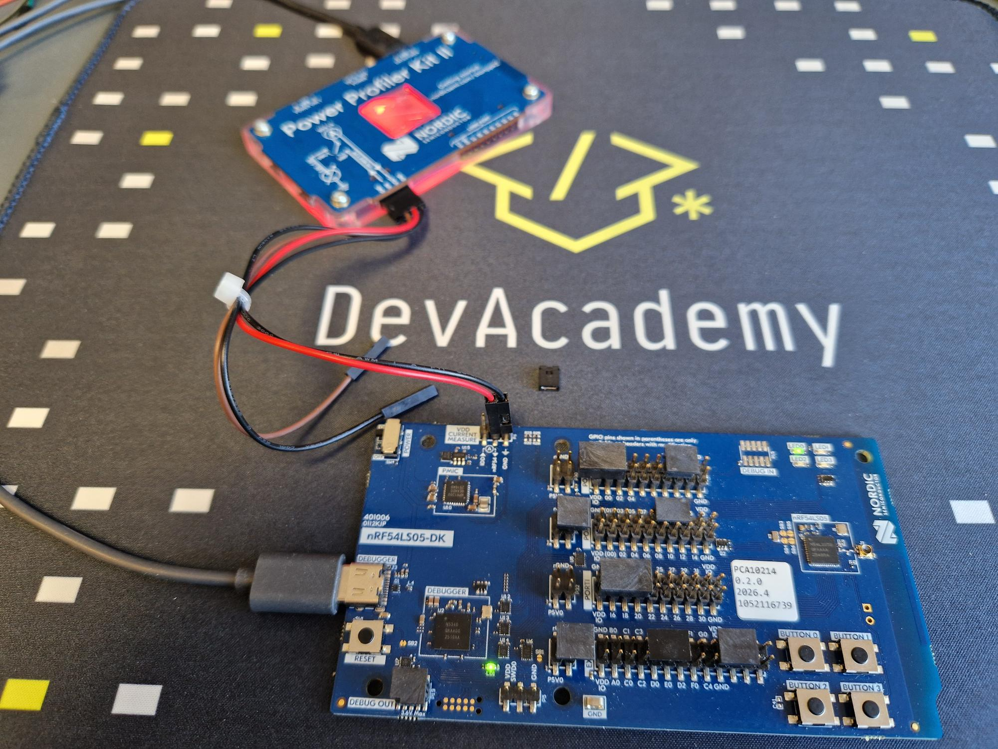
Remove the jumper on P6 (VDD CURRENT MEASURE), connect VOUT on the PPK2 to nRF54 on the P6 header (red cable in the image below) and GND to GND on the P6 header (black cable in the image below)
P6 close up on the nRF54LS05 DK
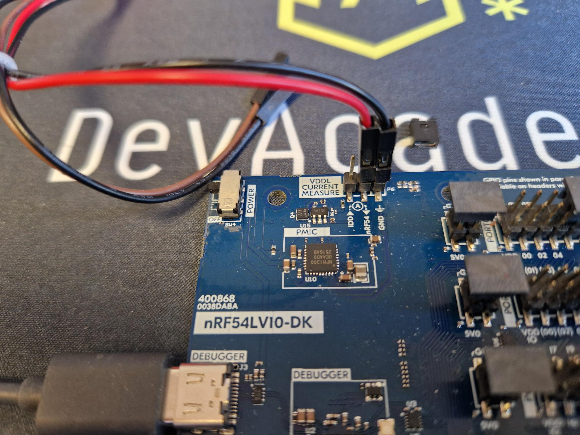
Remove the jumper on P6 (VDD CURRENT MEASURE), connect VOUT on the PPK2 to nRF54 on the P6 header (red cable in the image below) and GND to GND on the P6 header (black cable in the image below)
P6 close up on the nRF54LV10 DK
Important
Warning!
The nRF54LV10 SoC can support a voltage range of 1.2 to 1.7. Make sure you do not go above the max operating voltage, as this may damage the chip.
1.3 Select the PPK2 in the drop-down menu under Select Device.
Make sure your PPK2 is connected to your computer via a micro-USB cable and turned on.
Use the USB DATA/POWER line to power the device.
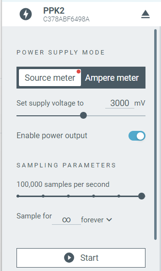
1.4 Select source meter mode, set the supply voltage to 3000 mV, and enable power output(The LED on the PPK2 should be red, indicating it’s in source mode).
We typically want to set the supply voltage to 3V, as this matches the datasheet numbers. But you can choose another voltage within the operating range for the chip.
Important
Warning!
Make sure you do not exceed the maximum operating voltage, as this may damage the chip.
If you choose to use ampere meter mode, note that the default voltage on the DK is 1.8V. So these measurements will not match your 3V source meter mode measurements.
It is important to click “enable power output” before flashing firmware to the DK, and starting the measurements. You can toggle this switch after programming in order to do a power cycle. Also if you want to restart your test, this is a convenient way of power cycling the chip.
2. Flash firmware to the DK.
First we will start by programming a pre-compiled hex file, so that we are sure that there is nothing wrong with the firmware.
If you are doing this on a custom board, you might get increased current consumption when running this hex, because external components are not initialized correctly. If that is the case, you can look at the code provided in step 4, and compile your own firmware, with the necessary devicetree/GPIO configurations.
Download the hex file available in the course GitHub repository
Download the hex file available in the course GitHub repository
Download the hex file available in the course GitHub repository
Download the hex file available in the course GitHub repository
You can program the hex using the nrfutil command line tool (CLI):
nrfutil device program --firmware <hexfile>
Or you can use the Programmer app:
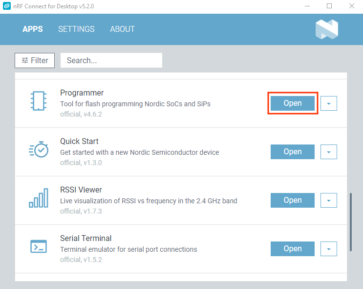
2.0 Open nRF Connect for Desktop, and launch the Programmer desktop application.
nRF Connect for Desktop
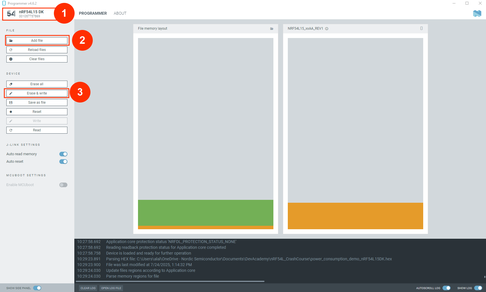
2.1 From the Select Device menu, choose your nRF54L DK (nRF54L15 DK, nRF54LM20 DK, nRF54LS05 DK, nRF54LV10A DK), then click on Add file. Select the binary file downloaded in the step 1.2.
2.2 Click Erase & write.
Programmer app available through nRF Connect for Desktop
Programmer app available through nRF Connect for Desktop
2.3 Examine the log. On a successful write, you should see a log similar to the following:
 INFO Writing HEX to Application core
 INFO Writing HEX to Application core 0%
 INFO Writing HEX to Application core 50%
 INFO Writing HEX to Application core 50%
 INFO Writing HEX to Application core 63%
 INFO Writing HEX to Application core 75%
 INFO Writing HEX to Application core 88%
 INFO Writing HEX to Application core 100%
 INFO Writing HEX to Application core completed
 INFO Reading memory for Application core
 INFO Reading memory for Application core 0%
 INFO Reading memory for Application core 100%
 INFO Reading memory for Application core completed
 INFO Parse memory regions for Application core
 DEBUG Sending event "programmer: running nrfutil device"
 DEBUG Sending event "programmer: running nrfutil device"
 DEBUG Sending event "programmer: running nrfutil device"
 INFO Reading readback protection status for Application core
 INFO Reading readback protection status for Application core 0%
 INFO Reading readback protection status for Application core 100%
Terminal
Close the Programmer app.
Always do a power cycle after programming to be sure that the device is no longer in debug mode.
3. Measure System OFF.
Start the measurement and observe the average current over a longer time period. > 10 seconds.
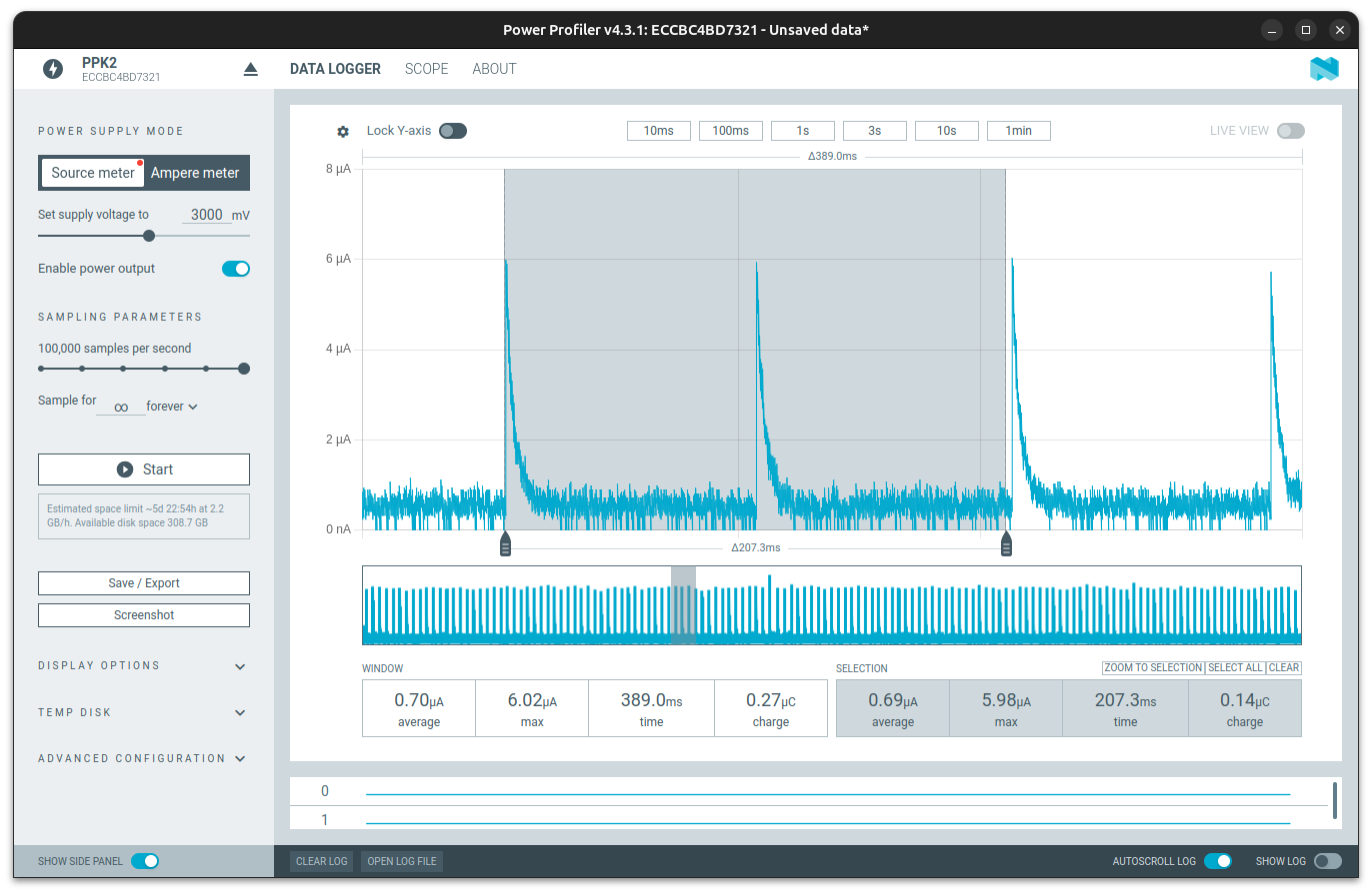
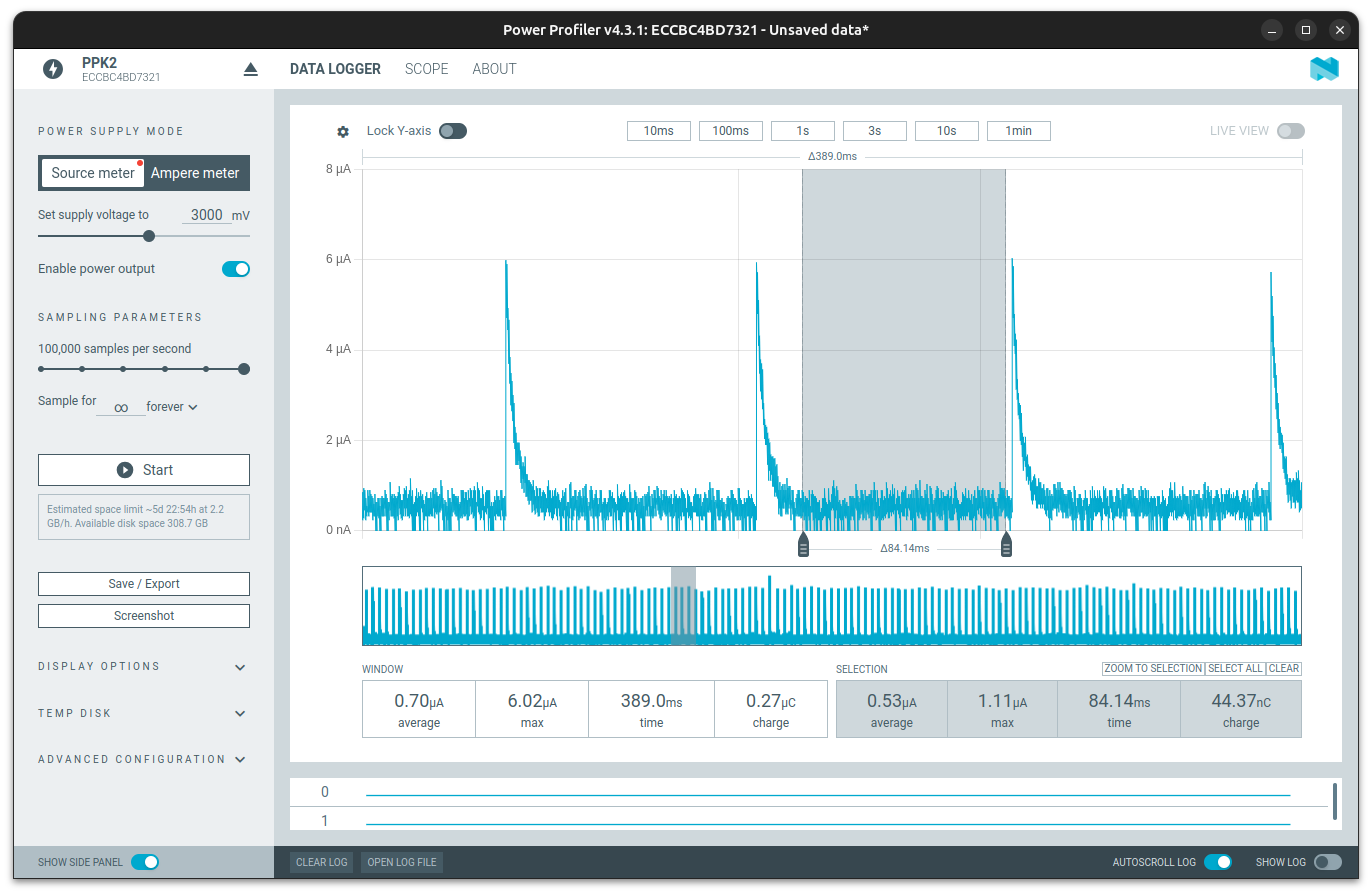
Here is a measurement conducted on the nRF54L15 DK, using the Power Profiler Kit:
Verify that the average current over a longer period matches the datasheet number:
IOFF0
System OFF, Wake on pin, 0 KB RAM retained
0.7 μA
If we want to investigate the current profile in more details we can first try to recognize the refresh spikes. In System OFF mode we would expect a spike period of 100 to 200 ms, according to what we discussed in the Measurement setup validation and error mitigation section.
Here is a plot selecting the area which covers two refresh spike periods:
The current is consumed in periodic bursts, meaning that we need to treat this as a periodic signal. The distance between the cursors should be a multiple of the periodic signal, as shown in the plot above, as discussed in the periodic signal and extrapolating data section.
Observe that the average current including only a few refresh spikes is the same as the average current over a longer time period, if we place the cursors correctly.
Also observe that the floor current between the spikes is 0.5 uA. This is the lowest we can have, as some current is also consumed by the chip itself directly on VDD. If we had leakage current on VDD from external components or through GPIOs, this floor current would have been increased, while keeping the same refresh spike distance. We will investigate this scenario in step 4.
So what information have we extracted from our measurements so far?
We have a periodic signal with a period of about 100ms → Indicating we are in System OFF
We have very low leakage on VDD → Floor current is < 0.5uA. Our measurement setup is good.
Below is a code snippet that can be used if you want to compile your own System OFF sample. This is useful if you are using a custom board with it’s own devicetree. The devicetree will set the GPIO configuration, and it will be retained in System OFF.
The easiest way to create your own System OFF firmware is to start with the zephyr/samples/hello_world sample, compile it, and make sure that it runs and prints to the console. Then we will add the code below.
4.1 Turn off the UART logger module and enable support for System power off.
First we want to turn off the UART logger module by adding CONFIG_SERIAL=n in the prj.conf file. While System OFF will turn off the UART as well, it will not reconfigure the GPIOs. During System OFF mode, the GPIO pins will retain their configured state. So if we do not turn off the UART through CONFIG_SERIAL=n, we will get some leakage through the GPIOs.
We also want to enable support for System power off, through enabling CONFIG_POWEROFF.
Add the following lines to the prj.conf file
Copy
CONFIG_SERIAL=n# Do not initialize UART logger moduleCONFIG_POWEROFF=y# System OFF library
Kconfig
4.2 Turn off the low frequency clock, RAM sections for CRACKEN and ICACHE and enter System OFF.
Then, in main.c, we want to turn off the low frequency clock and the GRTC through the sys_clock_disable() call, otherwise these will run in System OFF and consume around 0.2 uA. This is only relevant for the nRF54 series, as the previous series (nRF52/53) did not support RTC and LF clock in System OFF.
An additional NRF_MEMCONF->POWER[1].RET &= ~0xE is added, as we can turn off RAM sections 33, 34 and 35 as well, since we do not need these for our experiment. These sections are not covered by the sys_poweroff() call, and need to be switched off manually. This will reduce our current with another 0.3 uA.
Please refer to table 1 in the following link for more information on these RAM sections: Technical Documentation. Memory retention is covered in depth in lesson 5.
Replace the contents of main.c with the following code snippet
Copy
#include<stdio.h>#include<zephyr/kernel.h>#include<zephyr/sys/poweroff.h>#include<zephyr/drivers/timer/system_timer.h>intmain(void){//Turn off GRTC and LF clock:sys_clock_disable();//Turn off RAM sections for CRACKEN and ICACHE:NRF_MEMCONF->POWER[1].RET &= ~0xE; /* STEP 5 - Increase VDD leakage *///Enter System OFF:sys_poweroff();return0;}
C
4.3 Build and flash the sample to your DK.
Verify that you have the same current consumption as with the pre-compiled hex.
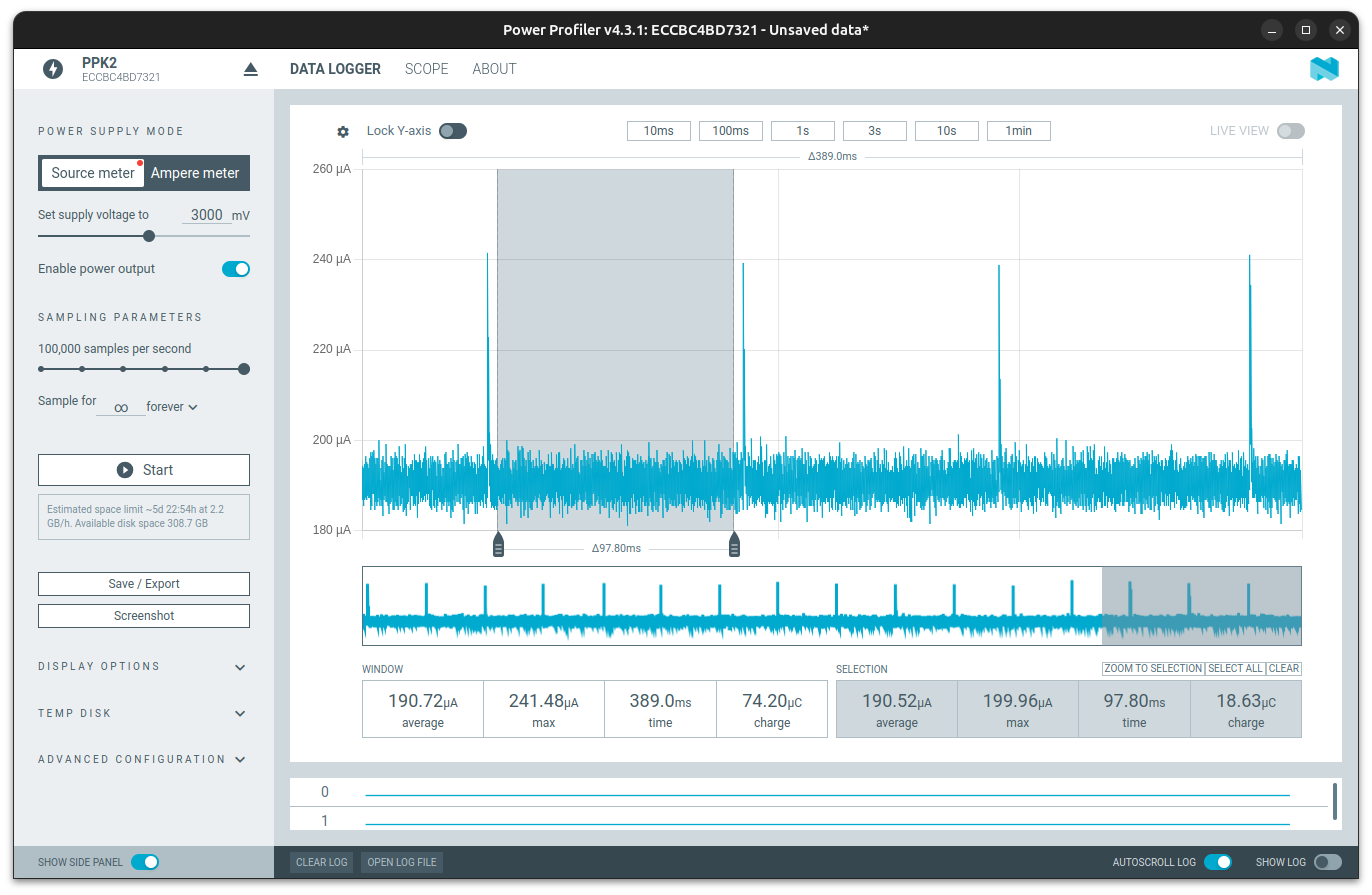
5. Increase and investigate VDD leakage.
If we want to investigate this scenario of having a leakage on VDD, and correlate this with our measurements, we can add the following code to our main() function, right above the sys_poweroff() call:
Copy
NRF_P0->PIN_CNF[4] = 0xD; // Set P0.04 as output with a pullup to VDDNRF_P0->OUTCLR = 1<<4; // Set P0.04 output to low (GND)
C
What this does is set the pin a low output. But we also configure a pullup to VDD. This means that current will flow directly from VDD through the pullup, down to GND.
This is usually not a valid configuration for an application, but we will use this configuration just for the purpose of showing an increased VDD current.
The internal pullup resistor on each GPIO is specified to be between 12 kOhm and 16 kOhm. In this example we set VDD to 3V, so we would expect a current of 188 uA to 250 uA flowing directly on the VDD domain.
Here is a plot showing how the VDD floor current has increased to 190 uA, but the refresh spike period stays at the same 100ms, as in our previous measurements, meaning that we are still in System OFF, but are having a 190 uA leakage on VDD
6. Measure System ON IDLE.
Remove the sys_clock_disable(), pin configuration and sys_poweroff() from main.c, and observe that we are now in System ON IDLE.
Remove or comment out the contents of main() so it looks like this
Copy
intmain(void){return0;}
C
Running this over a longer time period, we get an average current of ~2.45 uA
The expected current consumption running on nRF54L15 can be found in the datasheet under this scenario:
ION_IDLE8
System ON, Wake on pin + GRTC, LFXO, 256 KB RAM retained
2.9 μA
This is the default idle configuration in Zephyr, since we now have GRTC running from LFXO as our system timer, and the default full RAM retention.
Note that the RAM retention current is varying from device to device, and the the datasheet lists the typical value, as we discussed in this section. In this context it means that in reality the value has a normal distribution and that the typical value is the mean value across all devices. So if your measurement doesn’t match 100%, this is the reason. And that is also why we wanted to confirm our measurement setup with System OFF first.
We should further investigate the current profile, confirming that the refresh spike period is now much shorter than our System OFF measurements, due to the internal current draw is now much higher.
Now that we’ve confirmed our measurement setup is correct and we’re seeing the correct idle current, we’ll continue to the next lesson, where we add Bluetooth LE advertising to our application.
Nordic Developer Academy Privacy Policy
1. Introduction
In this Privacy Policy you will find information on Nordic Semiconductor ASA (“Nordic Semiconductor”) processes your personal data when you use the Nordic Developer Academy.
References to “we” and “us” in this document refers to Nordic Semiconductor.
2. Our processing of personal data when you use the Nordic Developer Academy
2.1 Nordic Developer Academy
Nordic Semiconductor processes personal data in order to provide you with the features and functionality of the Nordic Developer Academy. Creating a user account is optional, but required if you want to track you progress and view your completed courses and obtained certificates. If you choose to create a user account, we will process the following categories of personal data:
Email
Name
Password (encrypted)
Course progression (e.g. which course you have completely or partly completed)
Certificate information, which consists of name of completed course and the validity of the certificate
Course results
During your use of the Nordic Developer Academy, you may also be asked if you want to provide feedback. If you choose to respond to any such surveys, we will also process the personal data in your responses in that survey.
The legal basis for this processing is GDPR article 6 (1) b. The processing is necessary for Nordic Semiconductor to provide the Nordic Developer Academy under the Terms of Service.
2.2 Analytics
If you consent to analytics, Nordic Semiconductor will use Google Analytics to obtain statistics about how the Nordic Developer Academy is used. This includes collecting information on for example what pages are viewed, the duration of the visit, the way in which the pages are maneuvered, what links are clicked, technical information about your equipment. The information is used to learn how Nordic Developer Academy is used and how the user experience can be further developed.
2.2 Newsletter
You can consent to receive newsletters from Nordic from within the Nordic Developer Academy. How your personal data is processed when you sign up for our newsletters is described in the Nordic Semiconductor Privacy Policy.
3. Retention period
We will store your personal data for as long you use the Nordic Developer Academy. If our systems register that you have not used your account for 36 months, your account will be deleted.
4. Additional information
Additional information on how we process personal data can be found in the Nordic Semiconductor Privacy Policy and Cookie Policy.
Nordic Developer Academy Terms of Service
1. Introduction
These terms and conditions (“Terms of Use”) apply to the use of the Nordic Developer Academy, provided by Nordic Semiconductor ASA, org. nr. 966 011 726, a public limited liability company registered in Norway (“Nordic Semiconductor”).
Nordic Developer Academy allows the user to take technical courses related to Nordic Semiconductor products, software and services, and obtain a certificate certifying completion of these courses. By completing the registration process for the Nordic Developer Academy, you are agreeing to be bound by these Terms of Use.
These Terms of Use are applicable as long as you have a user account giving you access to Nordic Developer Academy.
2. Access to and use of Nordic Developer Academy
Upon acceptance of these Terms of Use you are granted a non-exclusive right of access to, and use of Nordic Developer Academy, as it is provided to you at any time. Nordic Semiconductor provides Nordic Developer Academy to you free of charge, subject to the provisions of these Terms of Use and the Nordic Developer Academy Privacy Policy.
To access select features of Nordic Developer Academy, you need to create a user account. You are solely responsible for the security associated with your user account, including always keeping your login details safe.
You will able to receive an electronic certificate from Nordic Developer Academy upon completion of courses. By issuing you such a certificate, Nordic Semiconductor certifies that you have completed the applicable course, but does not provide any further warrants or endorsements for any particular skills or professional qualifications.
Nordic Semiconductor will continuously develop Nordic Developer Academy with new features and functionality, but reserves the right to remove or alter any existing functions without notice.
3. Acceptable use
You undertake that you will use Nordic Developer Academy in accordance with applicable law and regulations, and in accordance with these Terms of Use. You must not modify, adapt, or hack Nordic Developer Academy or modify another website so as to falsely imply that it is associated with Nordic Developer Academy, Nordic Semiconductor, or any other Nordic Semiconductor product, software or service.
You agree not to reproduce, duplicate, copy, sell, resell or in any other way exploit any portion of Nordic Developer Academy, use of Nordic Developer Academy, or access to Nordic Developer Academy without the express written permission by Nordic Semiconductor. You must not upload, post, host, or transmit unsolicited email, SMS, or \”spam\” messages.
You are responsible for ensuring that the information you post and the content you share does not;
contain false, misleading or otherwise erroneous information
infringe someone else’s copyrights or other intellectual property rights
contain sensitive personal data or
contain information that might be received as offensive or insulting.
Such information may be removed without prior notice.
Nordic Semiconductor reserves the right to at any time determine whether a use of Nordic Developer Academy is in violation of its requirements for acceptable use.
Violation of the at any time applicable requirements for acceptable use may result in termination of your account. We will take reasonable steps to notify you and state the reason for termination in such cases.
4. Routines for planned maintenance
Certain types of maintenance may imply a stop or reduction in availability of Nordic Developer Academy. Nordic Semiconductor does not warrant any level of service availability but will provide its best effort to limit the impact of any planned maintenance on the availability of Nordic Developer Academy.
5. Intellectual property rights
Nordic Semiconductor retains all rights to all elements of Nordic Developer Academy. This includes, but is not limited to, the concept, design, trademarks, know-how, trade secrets, copyrights and all other intellectual property rights.
Nordic Semiconductor receives all rights to all content uploaded or created in Nordic Developer Academy. You do not receive any license or usage rights to Nordic Developer Academy beyond what is explicitly stated in this Agreement.
6. Liability and damages
Nothing within these Terms of Use is intended to limit your statutory data privacy rights as a data subject, as described in the Nordic Developer Academy Privacy Policy. You acknowledge that errors might occur from time to time and waive any right to claim for compensation as a result of errors in Nordic Developer Academy. When an error occurs, you shall notify Nordic Semiconductor of the error and provide a description of the error situation.
You agree to indemnify Nordic Semiconductor for any loss, including indirect loss, arising out of or in connection with your use of Nordic Developer Academy or violations of these Terms of Use. Nordic Semiconductor shall not be held liable for, and does not warrant that (i) Nordic Developer Academy will meet your specific requirements, (ii) Nordic Developer Academy will be uninterrupted, timely, secure, or error-free, (iii) the results that may be obtained from the use of Nordic Developer Academy will be accurate or reliable, (iv) the quality of any products, services, information, or other material purchased or obtained by you through Nordic Developer Academy will meet your expectations, or that (v) any errors in Nordic Developer Academy will be corrected.
You accept that this is a service provided to you without any payment and hence you accept that Nordic Semiconductor will not be held responsible, or liable, for any breaches of these Terms of Use or any loss connected to your use of Nordic Developer Academy. Unless otherwise follows from mandatory law, Nordic Semiconductor will not accept any such responsibility or liability.
7. Change of terms
Nordic Semiconductor may update and change the Terms of Use from time to time. Nordic Semiconductor will seek to notify you about significant changes before such changes come into force and give you a possibility to evaluate the effects of proposed changes. Continued use of Nordic Developer Academy after any such changes shall constitute your acceptance of such changes. You can review the current version of the Terms of Use at any time at https://academy.nordicsemi.com/terms-of-service/
8. Transfer of rights
Nordic Semiconductor is entitled to transfer its rights and obligation pursuant to these Terms of Use to a third party as part of a merger or acquisition process, or as a result of other organizational changes.
9. Third Party Services
To the extent Nordic Developer Academy facilitates access to services provided by a third party, you agree to comply with the terms governing such third party services. Nordic Semiconductor shall not be held liable for any errors, omissions, inaccuracies, etc. related to such third party services.
10. Dispute resolution
The Terms of Use and any other legally binding agreement between yourself and Nordic Semiconductor shall be subject to Norwegian law and Norwegian courts’ exclusive jurisdiction.
Switch language?
Progress is tracked separately for each language. Switching will continue from your progress in that language or start fresh if you haven't begun.
Your current progress is saved, and you can switch back anytime.
•Support for nRF54LS05 DK (Available through the early access sampling program) •Support for the nRF54LM20B with Axon NPU for Edge AI applications
Bluetooth LE updates
•Quality of Service module is now production-ready. •New experimental features for RF testing (Direct Test Mode) and low-latency packet handling (LE Flushable ACL).
MCUboot & Partition Manager
•Single-Slot DFU and RAM Load mode are both promoted to fully supported •Partition Manager is officially deprecated in favor of Zephyr's devicetree-based partitioning.