In this exercise, we will learn how to estimate the power budget of a Bluetooth LE device and its battery life without hardware.
Power budget estimation is the process of calculating the expected average power consumption of a device across all operational states and activities. It is typically performed during the design phase, before the hardware is finalized, to ensure components and power sources meet the device’s requirements and the desired battery life.
Doing a proper power budget estimation at the design phase can prevent costly late design iterations, enable informed trade-offs, and set realistic product expectations. One of the key pieces of information obtained from the power budget estimation is the choice of battery for the device.
We will use datasheet numbers and estimations from the Online Power Profiler to predict the device’s power consumption across its various operational states.
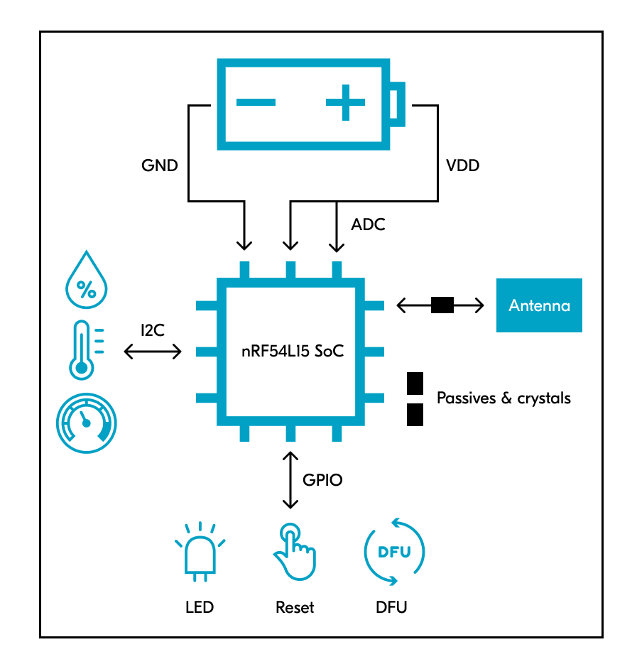
Device A
We will start with a simple device to understand the power budget estimation process. The device of choice is a wireless sensor device that broadcasts environmental sensor readings using Bluetooth LE. The device broadcasts the following data:
Temperature
Humidity
Air pressure
Battery voltage level
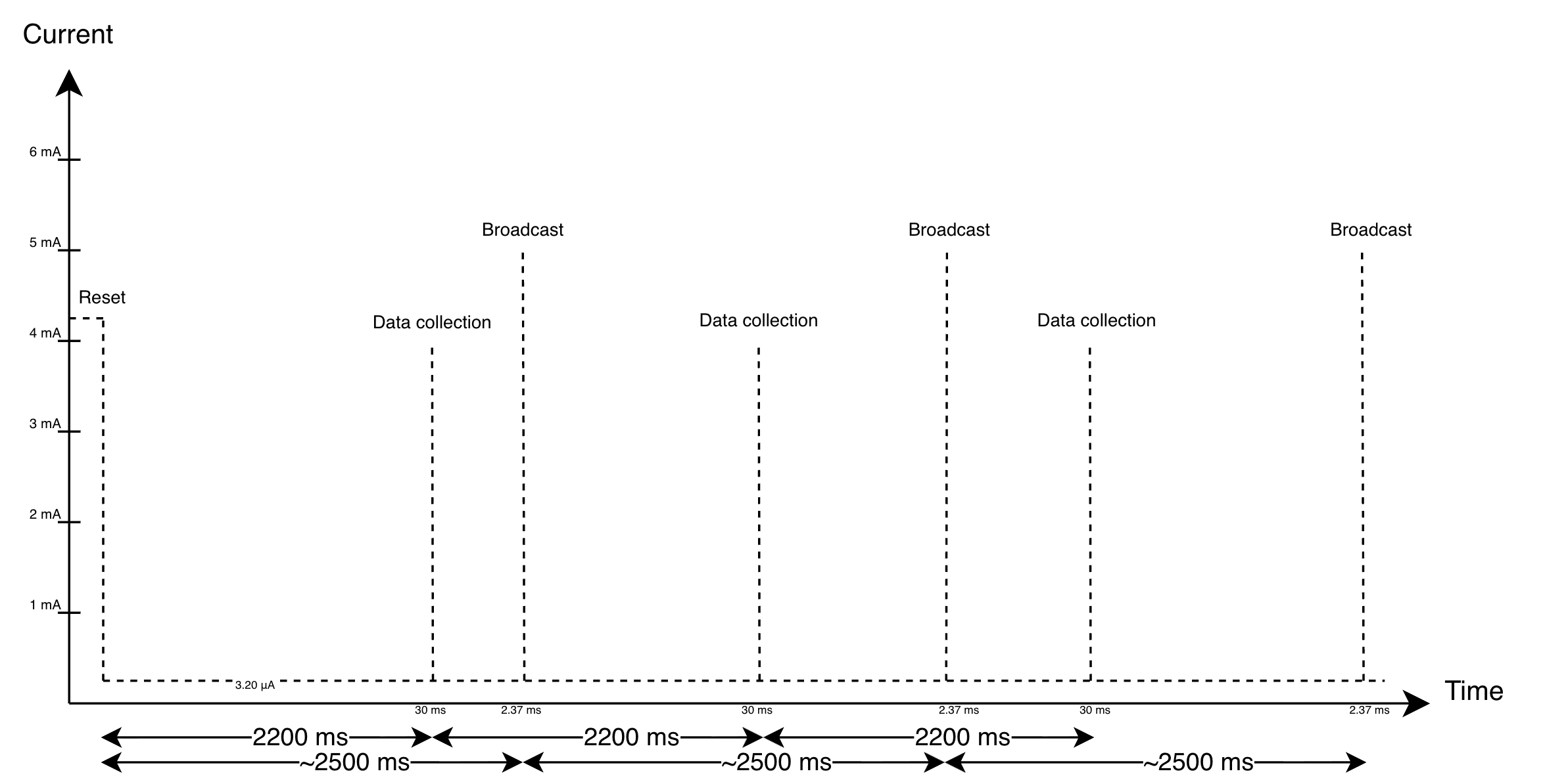
The device measures temperature, humidity, air pressure, and battery level every 2.2 seconds and broadcasts sensor data every 2.5 seconds.
Method of Bluetooth LE communication :
Primary: Broadcasting using legacy advertising
Secondary: Bluetooth LE Connection (ACL Connection)
The device’s primary communication method is broadcasting through legacy advertising (one-to-many). Device A uses this method because it requires no bidirectional communication. It simply broadcasts its reading, allowing other devices, such as a smartphone with an accompanying App, to act as a Bluetooth LE observer that displays and logs the readings.
Device A requires support for Over-the-Air Device Firmware Update, which can be triggered by holding the reset and boot buttons together. Once the device is in DFU mode, it uses Bluetooth LE Connection (ACL Connection) to receive the new firmware image.
Exercise steps
1. Obtaining device component power consumption.
In this step, we need to find out the power consumption of each component in the device in the different operational modes (for example, active mode, idle or sleep mode, etc.). We will assume that the device will be operating at a fixed voltage (for example, 3V) and only obtain the current consumption in µA or mA. These numbers are usually obtained from the datasheet of each component in your device’s bill of materials. However, some vendors provide tools that can help you simplify obtaining these numbers.
1.1 Wireless SoC
Our Device will be powered by the nRF54L15 SoC. The power consumption numbers of the SoC can be found in its datasheet in the electrical specification chapter. This chapter also includes current consumption scenarios showing typical current drawn from various use cases (for example, different peripherals’ current consumption).
Nordic Semiconductor offers the Online Power Profiler (OPP) on DevZone, a web tool that estimates the average current consumption of Nordic chips like the nRF52, nRF53, nRF54L, and nRF91 Series across various wireless protocols. It provides separate interfaces for Bluetooth LE, Matter over Thread, Wi‑Fi, and LTE‑M/NB‑IoT, allowing users to input parameters such as voltage, payload size, TX power, and interval timing. The OPP uses a statistical power model based on lab measurements—typically within ±5% error for reference boards—to estimate energy use per wireless event and idle power.
We will use the OPP to determine the estimated current consumption in the various operating modes of our device.
1.1.1 Broadcasting using legacy advertising
The architect chose legacy advertising as the primary communication method for their device. It meets the device’s requirements with the added bonus of providing backward compatibility with older devices.
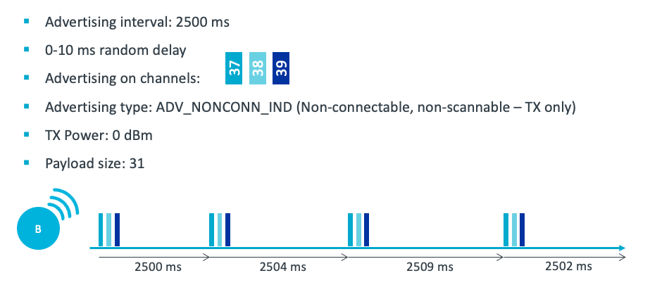
The device sends an advertising packet containing the data every ~ 2500 ms. As we discussed in the communication methods of Bluetooth LE, legacy advertising contains a random delay of 0 to 10 ms to reduce collisions on the primary advertising channels(# 37,38,39). We will refer to this as a Bluetooth LE event. The TX power is set to 0 dBm.
The same packet is actually sent over three different channels by default to maximize the chance of an observer receiving the packet. (Side note: the number of channels for advertising is firmware configurable from 1 to 3).
The payload in each packet uses the maximum size allowed in legacy advertising (31 bytes) to include sensor data (temperature, humidity, pressure) and battery voltage level. Each requires 2 bytes to represent the measured value, along with other manufacturer metadata, such as the FW version.
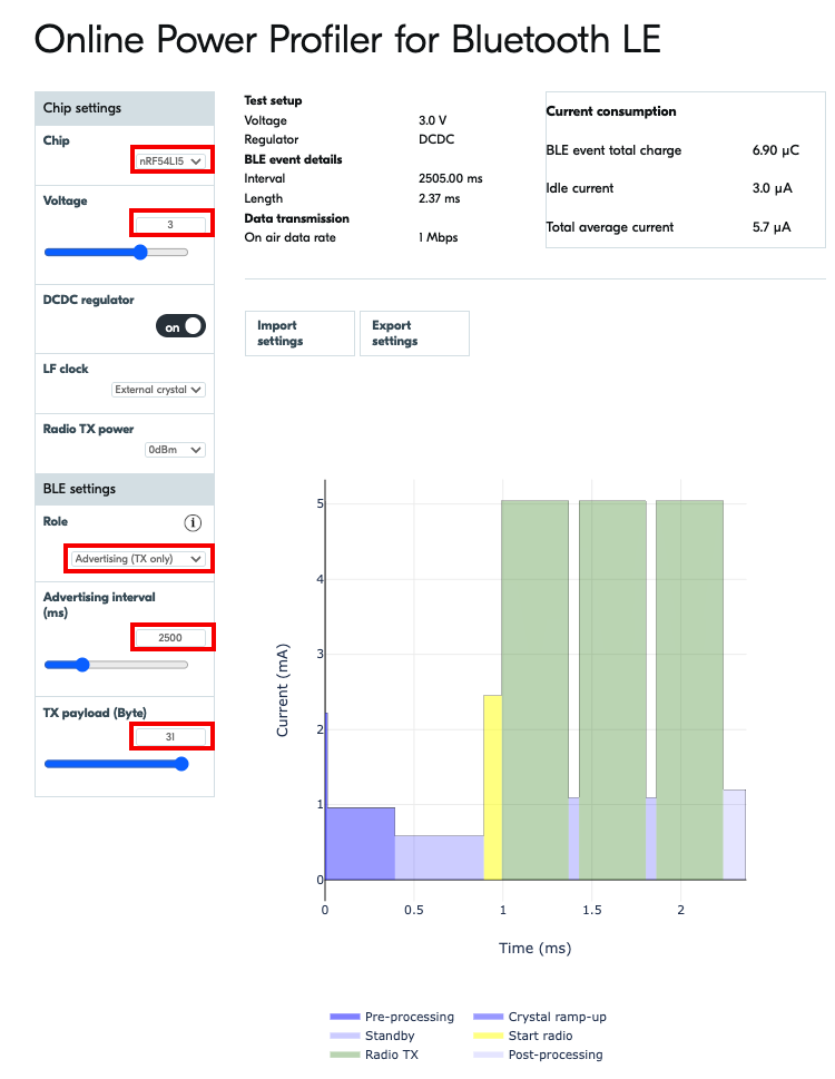
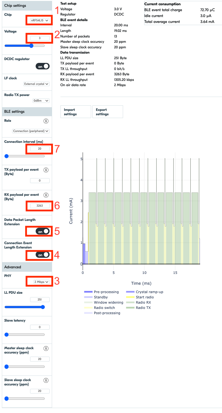
Now, if we go to the OPP site and enter these numbers as shown in the screenshot below:
The OPP provides reasonable estimates on:
The average current drawn during Bluetooth LE advertising events = BLE event total charge / BLE event length = 6.9μC / 2.37 ms = 2.911 mA. It is broken down into the following components as displayed by the tool:
Pre-processing: ~2.2 mA
Crystal ramp-up: ~1 mA
Start radio: ~2.4 mA (yellow spike)
Radio TX (x3 channels): ~5 mA (three green pulses)
Standby: ~ 0.6 – 1.1 mA
Post-processing: ~1.2 mA
The peak current consumed during the Bluetooth LE event: ~5 mA (Radio TX)
These numbers are estimates; however, in lesson 3 we will measure them with real hardware.
Please note that the total average current presented by the Online Power Profiler represents the Wireless SoC total average current with the sleep time between advertising events.
1.1.2 Bluetooth LE Connection (ACL Connection)
This is a secondary communication method for our device; it is used to support over-the-air Device Firmware Updates only.
The device must support over-the-air Device Firmware Updates for feature updates, improvements, bug fixes, and security patches. It uses an ACL connection to receive the firmware image from a central device (for example, smartphone). This update will not occur daily but approximately every X months, as explained in Step 2.
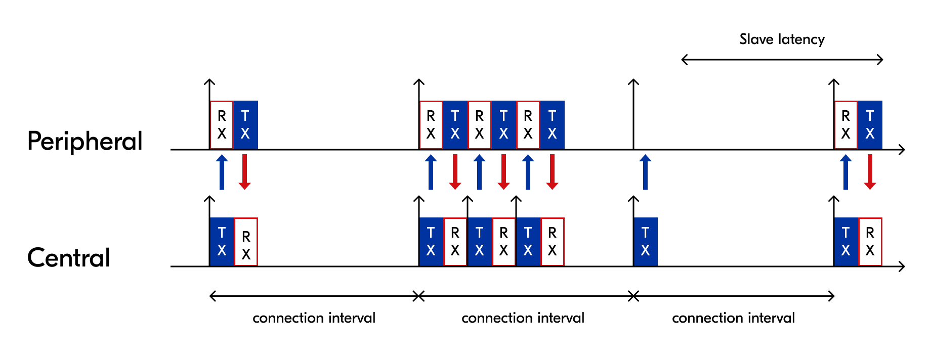
The device first advertises on all three primary channels (connectable advertising), each with an RX period waiting for a connection request from the central. Once it receives a connection request, the connection is established.
When in a connection, the central sends first, and the peripheral responds at an interval set by the central, which is the connection interval. One connection event can have multiple RX/TX pairs.
For transferring large data, such as a firmware image, the preference is usually to maximize throughput for faster firmware transfer. The connection parameters (covered in lesson 4) are set to reflect this (short connection interval, zero slave latency, Data Length Extension (DLE) enabled, 2M PHY).
As we can see from the OPP, the Bluetooth LE event associated with receiving a large amount of data from a central is relatively long (19.02 ms), and the average current consumption during that period is 3.64 mA. In addition, this event will occur multiple times to cover the entire firmware image.
If we compare the charge during the Bluetooth LE event for a high-data-rate connection vs. the charge during the Bluetooth LE event for legacy advertising, it’s ~10x.
1.1.3 CPU processing and peripherals
The CPU wakes up every 2200 ms to trigger reading the sensor connected via TWIM (I2C-compatible), sleep until the data is received, once sensor data is received, it will use the built-in Analog-to-Digital Converter (SAADC) to get the voltage level of the connected battery. This informs the peer device if a battery replacement is needed. It is cost-effective but less accurate than the dedicated fuel gauge solution in our PMIC family. Once the CPU has collected both the sensor and battery level, it then goes back to sleep.
Now, let’s estimate the current drawn by the CPU and peripherals in our device.
CPU:
The average current drawn by the Cortex ARM M33 CPU @ 128MHz on the nRF54L15 is documented in the datasheet as IAPPCPU0 and is equal to 2.6 mA (Cache enabled). Since our application has simple processing requirements and only coordinates peripherals without advanced algorithms or heavy processing tasks, the CPU will run for relatively very short periods.
TWIM:
The ballpark average current draw by the TWIM peripheral on the nRF54L15 SoC is ~ 250μA (depends on configuration and which domain the TWIM instance belongs to). The duration for sampling the sensor will depend on the sensor type and its configuration. We will calculate it in step 1.2.
SAADAC:
The current drawn by the SAADC is ~ 1.4 mA.
The duration of the SAADC voltage sample would depend heavily on the selected configurations. However, it’s a short period of few microseconds.
During the event of sampling the sensor and the battery voltage, we will assume that 1.5% of the time is spent by the CPU, 10% of the time is spent in TWIM transactions, 0.05% of the time is spent in SAADAC, and the rest of the time the CPU will be asleep.
Average Wireless SoC current consumption during data collection = 0.15/10 × 2.6 mA + 1.0/10 × 250 µA + 0.005/10 × 1.4 mA + 8.845/10 × 3 µA = 67.35 µA
1.1.4 Sleep
The sleep current of the nRF54L15 SoC can be obtained from the datasheet and it depends on the several parameters (for example, memory retention, wakeup sources, active peripheral, temperature, etc.) as we will see in lesson 5. However, on full memory retention, it is about 3 μA at room temperature.
nRF54L15 SoC modes in Device A
Component
Mode
Estimated average current
Interval
Comment
nRF54L15 SoC
Radio TX
2.911 mA
2500 ms
Broadcasting using legacy advertising
nRF54L15 SoC
Radio TX/RX
3.70 mA
20 ms
Receiving a firmware image from a central
nRF54L15 SoC
CPU + Peripheral(s)
67.35 µA
2200 ms
nRF54L15 SoC
Sleep
3 μA
–
1.2 Environmental sensor
The device will host a combined temperature, humidity and pressure sensor that will be sampled every 2200 ms. For a sensor of this type it usually consumes between 340- 714 μA during measurements and about 0.1 – 0.2 μA in sleep. An example sensor is the BME280.
Component
Mode
Estimated average current
Interval
Comment
BME280
Measurement (Forced mode)
527 μA
2200 ms
BME280
Sleep
0.1 μA
–
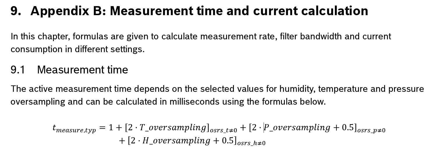
The duration of the measurement will heavily depend on the sensor settings ( mode of operation, oversampling, applied filters, etc.). Sensor vendors usually provide formulas to calculate it. For example, BME280 – datasheet – Chapter 9 specifies the following formula:
We can assume the following oversampling settings:
Temperature (8x): 2×8=16 ms
Pressure (4x): 2×4+0.5=8.5 ms
Humidity (2x): 2×2+0.5=4.5 ms
Total Typical Time (tmeasure,typ): 1+16+8.5+4.5= 30 ms
1.3 User interface
The device has two active-low push buttons, one for reset and one for making the device enter DFU mode if pressed together with the reset button. These buttons, as we covered previously in this lesson, consume zero current when they are not active.
A single active-low LED is available on the device. It remains off during device normal operation and sleep, activating only in DFU mode and consuming about 5 mA.
1.4PCB, passives, 2.4 GHz antenna, and other components
The device will include the necessary passive components (capacitors, inductors, crystals, resistor) as specified in the reference design of the nRF54L15 SoC. It will also include an antenna matching circuit and a 2.4 GHz antenna.
In addition to the components needed for the wireless SoC, it will include pull-up resistors for the I2C bus, potentially a load switch to couple a voltage divider on battery voltage measurements.
These components will have impact on the power consumption. For example, the decoupling capacitors type and quality will dictate how much leakage current they will have. For properly selected capacitors, the leakage current is negligible and in the order of few nano amps. However, keep in mind that on device power-up there will be a short transit period to charge these capacitor .
The quality of the PCB affects power consumption. For example, a poor-quality PCB with low-impedance points (solder flux residue, poor etching quality, etc..) between power and ground causes leakage current.
For this exercise, assume Device A’s passives and other components have a constant power leakage of 0.1 μA.
2. Establishing the device usage profile (device behavior over time).
A device usage profile defines the expected operational modes and their durations for a Bluetooth LE device over a representative time period, reflecting real-world user behavior and usage conditions.
2.1 In this step, we need to have a good picture of the device modes of operation over time. This is probably the most difficult step in the power budget calculation as it’s very much device dependent and user-behavior dependent.
For our simple device (Device A), the user interaction with the device is pretty much straightforward. The user turns on the device, mount it somewhere where he/she is interested in monitoring the temperature, humidity and pressure. Then, the user uses a dedicated app on his/her smartphone whenever he is interested in the reading. The app will also show a notification if a new firmware is available for the device, in this case the user puts the device in DFU mode and update it.
2.1.1 List the modes of operation for the device
For Device A, we have basically:
Data collection mode : The device polls data from the sensor and the battery voltage level.
Broadcast mode: The device transmits the readings as Bluetooth LE advertising packet.
Sleep mode: The device is in sleep mode.
DFU mode : The device is in DFU mode expecting a new firmware image from a central device (example – a smartphone).
2.1.2 For each of the modes, you need to have an estimation of the average current in that mode, we will use the numbers collected in step 1 for this. In addition to the average current, you need to have an estimation on the duration of these modes.
We will start with the first three modes since they represent the normal “dominating” operation of the device. Let’s see what’s happening in 1 minute of device normal operation:
We have 60/2.2 = 27.2 data collection events. Each is about 30,0135 ms in duration
We have 60/2.4 = 24 Bluetooth LE broadcast events. Each is about 2.37 ms in duration.
Mode
Peak current estimation (mA)
Average current consumption estimation (μA)
Duration (ms)
Duty cycle percentage
Data collection
CPU+SAADC (2.6+1.4) = 4
67.35 + 527 = 594,35
(30+0.0135)x27.27 = 818.50
1.3642%
Broadcast
Radio TX = 5
2911
2.37x 24 = 56.88
0.0948%
Sleep
0.0032
3 + 0.1 + 0.1 = 3.2
60000 – 818.5 – 56.88 = 59124.62
98.541%
Besides normal operation, the device will likely undergo DFU updates. We will assume 4 updates per year, one for each quarter. We will also assume that the duration of the complete DFU process is 36 seconds (entering DFU, receiving a new image, validating image, rebooting). We will assume that the average current consumption during a DFU process is equal to 8.7 mA (Radio TX/RX + LED indication).
Even though sleep has the lowest current(3.2 µA), increasing it will have the most drastic impact on average current (calculated next) because it runs 98.541% of the time.
2.1.3 Calculate the total average current of the device
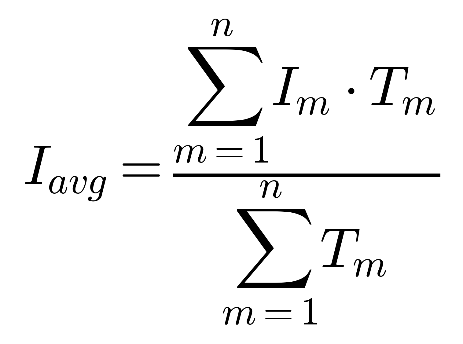
The total average current of the device can be calculated using the formula below:
I avg = Total Average current
n = Number of device operational mode
Im = Average current in mode m
Tm = Time spent in mode m
The total average current of the device will have a direct impact on the battery life of the device
Normal operation – calculated for 1 min of operation (Without DFU): I avg = ((594.35 µA × 818.5 ms + 2911 µA × 56.88 ms + 3.2 µA × 59124.62 ms) / 60000 ms) = 14.02µA
Let’s now calculate the average current during a quarter to include the impact of DFU
Selecting the battery type and size for a device is crucial, as it impacts the device’s size, cost, and overall user experience. We will break down the process of evaluating battery choices for our device into parts.
The first part focuses on defining selection priorities (for example, size, cost, and user experience).
The second part specifies the battery requirements, including capacity, voltage range, and tolerance to high peak currents. The third part estimates battery life for the selected choice.
3.1 Define battery selection priorities for your device
Given that our device (Device A) is intended to be a simple, low cost wireless sensor we will set the selection priorities as follows:
Small form factor. We want the device to be small in size and can fit or mounted in different places.
Low cost. To save cost the device should:
Not require external voltage regulators. Voltage range from the battery should match the voltages of used components
Preferably not going to use advanced PMIC features: fuel gauge, charging, etc..
Battery replacement should occur as infrequently as possible, preferably once every year or more.
3.2 Estimate device’s total average current, peak current, peak current duration
Through steps 1 and 2, we have already obtained two key numbers related to selecting a battery for our device. First is the total average current of the device (14.02 µA), the second number is the peak current of the device (8.7 mA). We have also obtained some information using the OPP on the duration of the peak current.
3.2 Determine required battery specifications
Every battery, regardless of its chemistry, has several common specifications that are usually specified in its datasheet:
Capacity: This is arguably the most critical battery specification. It represents the total energy stored in a battery, usually measured in mAh. For example, a 220 mAh battery can theoretically deliver 220 mA for 1 hour, 110 mA for 2 hours, or 1 mA for 220 hours. However, the actual usable capacity varies based on discharge rate, high current peaks (aka: high pulse drain), high current peaks duration, temperature, and other conditions. Therefore, Nominal and Effective capacity values provide more accurate specifications.
Nominal Capacity: This capacity reflects nominal conditions, typically at very low discharge rates like C/20 or C/10 at room temperature, this is stated in the datasheet as a typical drain. Each manufacturer specifies the conditions for this capacity, usually including temperature and current. For instance, a capacity of 235 mAh at 0.19 mA.
Effective Capacity: This is the actual capacity of the battery in your product or application. This capacity can be lower or higher than the nominal capacity depending on how your product uses the battery and temperature, which are the two main factors.
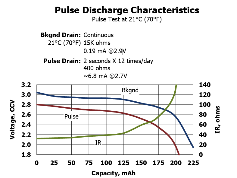
The most important thing to understand about batteries is that their actual or effective capacity isn’t usually a linear relationship with current draw. The actual capacity of one battery where the current drawn is 10 mA will be different than one where you’re drawing 10 uA. The less current you draw, the more capacity the battery will seem to have, beyond just the linear relationship because the battery is subjected to less stress from peak currents. This is important in Bluetooth LE applications where the average current is low, but the peak currents of Bluetooth LE radio transmissions are higher. This is documented in the battery datasheet through a Pulse Discharge figure or Internal Resistance Characteristics figure.
Let us take the example of the popular CR2032, which has the nominal capacity of 235 mAh. If we examine the pulse discharge diagram:
We can see it provides two tests both at the same temperature 21 °C:
Test 1 (Background (Bkgnd) load – blue line): continuous drain of ~0.19 mA at ~2.9 V. The effective capacity of the battery (~225) is very close to the nominal which is 235 mAh
Test 2 (Pulse drain load – red line): Pulses of 6.8 mA magnitude with 2 seconds width, at an interval of 12/day. The effective capacity of the device is reduced to 200 mAh.
Volume: The physical space a battery occupies, measured in cubic centimeters (cm³)
Voltage: The voltage profile of a battery is the output voltage your system sees over time. Different battery chemistries have different voltage profiles, which can make a big difference in your product design. Batteries have a nominal voltage, which is the voltage the battery has when it is fresh new and has no load. They also have a cutoff voltage (also called end-of-discharge voltage or minimum operating voltage), which is the lowest voltage at which a battery should be discharged before it is considered depleted or needs recharging/replacement. That is why some batteries specify their voltages in range (nominal voltage – cut voltage). For example, CR2032 has 3.0V- 2.0V.
we have the following options non-rechargeable batteries
The CR1620 has a voltage range of 3.0 V-2.0 V, making it suitable for a single battery to power our device (since our components require a voltage from 1.7 V-3.3 V), it also have a very compact volume of 0.4 cm3, however, the effective capacity would be around ~60 mAh which translates to < half-year battery life (formula covered in step 4).
While alkaline AA and AAA batteries are commonly available and straightforward to source, two cells must be connected in series to meet the component’s voltage requirements, resulting in a bulkier product form factor. Alternatively, if a single AA or AAA battery is preferred, a PMIC is required to boost the voltage, as covered in Lesson 2, Exercise 1 – Powering nRF54L devices from a single AA/AAA battery
A more fitting option on the list is the popular CR2032, which has a matching voltage for our system, a compact size, and an effective capacity that translates to over a year of battery life.
If more battery life is preferred over device size, consider high-capacity batteries like the CR2450 and CR123.
4. Estimate the battery life of the device.
4.1 Estimate the effective battery capacity for the selected battery
The battery of choice for our device is the CR2032 which has a nominal capacity of 235 mAh. Given that our device operates in a heavy sleep duty cycle of 99.7% and the high current peaks are happening at a relatively long intervals (2200 & 2500 ms) and for very short durations, we will assume that the effective battery capacity is 15% less than the nominal capacity due to drain pattern and differences in the temperature.
Assumed reduction in battery capacity = r = 15%
Effective Battery Capacity = 235 x (1 – 0.15) = ~ 200 mAh
4.2 Calculate the estimated battery life
Estimated Battery Life = 200 mAh / 0.01406 mA ≈ 14,225 hours ≈ 1.62 years
Optional Assignments
Part 1:
Assume that the designer decided to use the LED on the board so that it blinks 20 ms pulse every 2 seconds during device normal operation. What would be the new estimated battery life of the device given that the battery of choice is kept to the CR2032?
Part 2 (Device B):
Assume the designer upgraded the device to include an 8 MByte flash memory for logging sensor readings every minute. The device will use connectable advertising to broadcast its readings as before, with the option to accept connections from a central device to collect logged data. Repeat Steps 1 to 4 to calculate average total current, peak current, and evaluate battery options for over one year of battery life.
Nordic Developer Academy Privacy Policy
1. Introduction
In this Privacy Policy you will find information on Nordic Semiconductor ASA (“Nordic Semiconductor”) processes your personal data when you use the Nordic Developer Academy.
References to “we” and “us” in this document refers to Nordic Semiconductor.
2. Our processing of personal data when you use the Nordic Developer Academy
2.1 Nordic Developer Academy
Nordic Semiconductor processes personal data in order to provide you with the features and functionality of the Nordic Developer Academy. Creating a user account is optional, but required if you want to track you progress and view your completed courses and obtained certificates. If you choose to create a user account, we will process the following categories of personal data:
Email
Name
Password (encrypted)
Course progression (e.g. which course you have completely or partly completed)
Certificate information, which consists of name of completed course and the validity of the certificate
Course results
During your use of the Nordic Developer Academy, you may also be asked if you want to provide feedback. If you choose to respond to any such surveys, we will also process the personal data in your responses in that survey.
The legal basis for this processing is GDPR article 6 (1) b. The processing is necessary for Nordic Semiconductor to provide the Nordic Developer Academy under the Terms of Service.
2.2 Analytics
If you consent to analytics, Nordic Semiconductor will use Google Analytics to obtain statistics about how the Nordic Developer Academy is used. This includes collecting information on for example what pages are viewed, the duration of the visit, the way in which the pages are maneuvered, what links are clicked, technical information about your equipment. The information is used to learn how Nordic Developer Academy is used and how the user experience can be further developed.
2.2 Newsletter
You can consent to receive newsletters from Nordic from within the Nordic Developer Academy. How your personal data is processed when you sign up for our newsletters is described in the Nordic Semiconductor Privacy Policy.
3. Retention period
We will store your personal data for as long you use the Nordic Developer Academy. If our systems register that you have not used your account for 36 months, your account will be deleted.
4. Additional information
Additional information on how we process personal data can be found in the Nordic Semiconductor Privacy Policy and Cookie Policy.
Nordic Developer Academy Terms of Service
1. Introduction
These terms and conditions (“Terms of Use”) apply to the use of the Nordic Developer Academy, provided by Nordic Semiconductor ASA, org. nr. 966 011 726, a public limited liability company registered in Norway (“Nordic Semiconductor”).
Nordic Developer Academy allows the user to take technical courses related to Nordic Semiconductor products, software and services, and obtain a certificate certifying completion of these courses. By completing the registration process for the Nordic Developer Academy, you are agreeing to be bound by these Terms of Use.
These Terms of Use are applicable as long as you have a user account giving you access to Nordic Developer Academy.
2. Access to and use of Nordic Developer Academy
Upon acceptance of these Terms of Use you are granted a non-exclusive right of access to, and use of Nordic Developer Academy, as it is provided to you at any time. Nordic Semiconductor provides Nordic Developer Academy to you free of charge, subject to the provisions of these Terms of Use and the Nordic Developer Academy Privacy Policy.
To access select features of Nordic Developer Academy, you need to create a user account. You are solely responsible for the security associated with your user account, including always keeping your login details safe.
You will able to receive an electronic certificate from Nordic Developer Academy upon completion of courses. By issuing you such a certificate, Nordic Semiconductor certifies that you have completed the applicable course, but does not provide any further warrants or endorsements for any particular skills or professional qualifications.
Nordic Semiconductor will continuously develop Nordic Developer Academy with new features and functionality, but reserves the right to remove or alter any existing functions without notice.
3. Acceptable use
You undertake that you will use Nordic Developer Academy in accordance with applicable law and regulations, and in accordance with these Terms of Use. You must not modify, adapt, or hack Nordic Developer Academy or modify another website so as to falsely imply that it is associated with Nordic Developer Academy, Nordic Semiconductor, or any other Nordic Semiconductor product, software or service.
You agree not to reproduce, duplicate, copy, sell, resell or in any other way exploit any portion of Nordic Developer Academy, use of Nordic Developer Academy, or access to Nordic Developer Academy without the express written permission by Nordic Semiconductor. You must not upload, post, host, or transmit unsolicited email, SMS, or \”spam\” messages.
You are responsible for ensuring that the information you post and the content you share does not;
contain false, misleading or otherwise erroneous information
infringe someone else’s copyrights or other intellectual property rights
contain sensitive personal data or
contain information that might be received as offensive or insulting.
Such information may be removed without prior notice.
Nordic Semiconductor reserves the right to at any time determine whether a use of Nordic Developer Academy is in violation of its requirements for acceptable use.
Violation of the at any time applicable requirements for acceptable use may result in termination of your account. We will take reasonable steps to notify you and state the reason for termination in such cases.
4. Routines for planned maintenance
Certain types of maintenance may imply a stop or reduction in availability of Nordic Developer Academy. Nordic Semiconductor does not warrant any level of service availability but will provide its best effort to limit the impact of any planned maintenance on the availability of Nordic Developer Academy.
5. Intellectual property rights
Nordic Semiconductor retains all rights to all elements of Nordic Developer Academy. This includes, but is not limited to, the concept, design, trademarks, know-how, trade secrets, copyrights and all other intellectual property rights.
Nordic Semiconductor receives all rights to all content uploaded or created in Nordic Developer Academy. You do not receive any license or usage rights to Nordic Developer Academy beyond what is explicitly stated in this Agreement.
6. Liability and damages
Nothing within these Terms of Use is intended to limit your statutory data privacy rights as a data subject, as described in the Nordic Developer Academy Privacy Policy. You acknowledge that errors might occur from time to time and waive any right to claim for compensation as a result of errors in Nordic Developer Academy. When an error occurs, you shall notify Nordic Semiconductor of the error and provide a description of the error situation.
You agree to indemnify Nordic Semiconductor for any loss, including indirect loss, arising out of or in connection with your use of Nordic Developer Academy or violations of these Terms of Use. Nordic Semiconductor shall not be held liable for, and does not warrant that (i) Nordic Developer Academy will meet your specific requirements, (ii) Nordic Developer Academy will be uninterrupted, timely, secure, or error-free, (iii) the results that may be obtained from the use of Nordic Developer Academy will be accurate or reliable, (iv) the quality of any products, services, information, or other material purchased or obtained by you through Nordic Developer Academy will meet your expectations, or that (v) any errors in Nordic Developer Academy will be corrected.
You accept that this is a service provided to you without any payment and hence you accept that Nordic Semiconductor will not be held responsible, or liable, for any breaches of these Terms of Use or any loss connected to your use of Nordic Developer Academy. Unless otherwise follows from mandatory law, Nordic Semiconductor will not accept any such responsibility or liability.
7. Change of terms
Nordic Semiconductor may update and change the Terms of Use from time to time. Nordic Semiconductor will seek to notify you about significant changes before such changes come into force and give you a possibility to evaluate the effects of proposed changes. Continued use of Nordic Developer Academy after any such changes shall constitute your acceptance of such changes. You can review the current version of the Terms of Use at any time at https://academy.nordicsemi.com/terms-of-service/
8. Transfer of rights
Nordic Semiconductor is entitled to transfer its rights and obligation pursuant to these Terms of Use to a third party as part of a merger or acquisition process, or as a result of other organizational changes.
9. Third Party Services
To the extent Nordic Developer Academy facilitates access to services provided by a third party, you agree to comply with the terms governing such third party services. Nordic Semiconductor shall not be held liable for any errors, omissions, inaccuracies, etc. related to such third party services.
10. Dispute resolution
The Terms of Use and any other legally binding agreement between yourself and Nordic Semiconductor shall be subject to Norwegian law and Norwegian courts’ exclusive jurisdiction.
Switch language?
Progress is tracked separately for each language. Switching will continue from your progress in that language or start fresh if you haven't begun.
Your current progress is saved, and you can switch back anytime.
•Support for nRF54LS05 DK (Available through the early access sampling program) •Support for the nRF54LM20B with Axon NPU for Edge AI applications
Bluetooth LE updates
•Quality of Service module is now production-ready. •New experimental features for RF testing (Direct Test Mode) and low-latency packet handling (LE Flushable ACL).
MCUboot & Partition Manager
•Single-Slot DFU and RAM Load mode are both promoted to fully supported •Partition Manager is officially deprecated in favor of Zephyr's devicetree-based partitioning.