The nRF54L Series has up to 4xstandard UART peripherals and one high-speed UART peripheral.
High-speed UART: The high-speed UART instance is placed in the MCU power domain and operates on a 128 MHz clock, enabling baud rates up to 4 Mbps.
Standard UART: The standard UARTs are located in the peripheral and low-power domains and operate on a 16 MHz clock, supporting baud rates up to 1 Mbps.
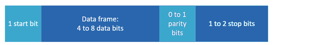
Flexible frame size
The UART peripherals support programmable data frame sizes from 4 to 8 bits with optional hardware-generated parity bits.
Figure 1. UART frame with flexible data length
Address filtering
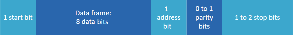
The nRF54L Series UART supports address filtering. This functionality allows the receiver to be configured to ignore any data frames that are not addressed to it. In this mode, a 9-bit frame size is used, consisting of 8 data bits plus 1 address bit. The value of the address bit determines the interpretation of the preceding 8; if the address bit is 0, the bits are treated as data; if it is 1 they are recognized as the address.
Figure 2. UARTE frame with fixed data length
Additionally, the UART peripheral instances support the following features:
Full-duplex operation with easyDMA transfer in both directions
Serial Peripheral Interface (SPI) – controller and target
The nRF54L Series SoC is equipped with SPI controller and target peripheral instances. Similarly to UART, one instance is connected to the MCU power domain, operating on a 128 MHz clock frequency, with a maximum speed of 32MHz. The remaining instances are located in the peripheral and low power domains, operating on a 16 MHz clock frequency, with a maximum speed of 8MHz.
DCX functionality
Outgoing transfer from an SPI controller can be divided into command and data bytes. For targets requiring an additional signal to differentiate these segments, the SPI peripheral automatically generates it.
Figure 3. D/CX example
Chip select (CSN) hardware control
The SPI controller offers the capability to automatically control the CSN pin during data transfers. Additionally, SPI supports the following features:
EasyDMA
SPI modes 0 to 3
Semaphore – Prevents simultaneous access to data buffers by the SPI target and the CPU.
I2C compatible two-wire interface (TWI) – controller and target
The two-wire interface facilitates half-duplex serial communication, allowing a controller (TWIM) to interact with individually addressed targets (TWIS) on the same bus. This setup supports communication with up to 127 targets.
Figure 4. Typical TWI setup with one controller and three targets
The nRF54L Series has up to four TWI controller/target instances. Both the controller and the target share the following features:
I2C compatibility
Variable bit rates – Supports 100 kbps, 400 kbps, and 1000 kbps bit rate depending on the selected pull-up resistor and bus capacitance combinations.
Clock stretching support
EasyDMA usage
Note
Note on Serial Interfaces (SPIM/SPIS/TWIM/TWIS/UARTE)
Each serial interface peripheral within the nRF54L Series is uniquely identified by an ID, and only one peripheral with a given ID can be active at any time. This is due to the fact that peripherals sharing the same ID also share the same hardware resources, including the base address and register set in the memory map.
For example, if you are using UARTE20, you cannot simultaneously use SPIM20, SPIS20, TWIM20, or TWIS20, as they all share ID 20. However, peripherals with different IDs operate independently because they have separate base addresses and register sets. For instance, while UARTE20 is active, you can still use: • UARTE21 • SPIM21 / SPIS21 • TWIM21 / TWIS21 • Any other serial peripheral with a different ID than 20.
Inter-IC sound interface (I2S)
The I2S in the nRF54L Series SoC supports both target and controller modes. Additionally, thanks to two data lines (SDIN, SDOUT), it allows simultaneous bidirectional (TX and RX) audio streaming. The I2S can only be used with physical pins from port P1.
In controller mode, the master clock (MCK) is crucial as it is the source from which the left-right clock (LRCK) and the serial clock (SCK) are derived. The master clock generator must always be active in controller mode.
Additionally, the master clock generator can be enabled in target mode. This is particularly useful if the external controller lacks the capability to generate its own master clock, ensuring consistent and reliable operation across different configurations.
The I2S peripheral in the nRF54L Series SoC supports a variety of sample widths, allowing selection from 8, 16, 24, or 32 bits:
I2S format – In this format, each audio frame consists of a pair of samples, one for the left channel, one for the right channel, or both. The left sample is transmitted during the low half period of the LRCK, and the right sample is transmitted during the high half period of LRCK.
Figure 5. I2S format. Identical sample width and half-frame width. Left sample on low level of LRCK
Aligned format – In this format, each audio frame consists of a pair of samples, one for the left channel, one for the right channel, or both. The left sample is transferred during the high half period of LRCK, followed by the right sample during the low half period of LRCK. When the half-frame sample width is longer than the sample width, the sample can be aligned to the left or right side.
Figure 6. Data aligned to the left side
Figure 7. Data aligned to the right side
Like many other peripherals, the I2S module utilizes easyDMA for audio data transfer, allowing operations without CPU involvement.
Note: In nRF54LM20 the I2S peripheral has been superseded by the TDM peripheral
Pulse density modulation interface (PDM)
The PDM module in the nRF54L Series is designed to sample pulse density modulated signals, which are typically generated from external audio frontends like digital microphones. It features a configurable microphone clock output, adjustable within the range of 768 kHz to 2.56 MHz.
Samples are coded to digital form using Pulse Code Modulation (PCM) with additional decimation filtering. Storing in the RAM memory without CPU involvement allows for continuous audio streaming.
In addition, the PDM peripheral can be configured to sample on both edges of the clock signal, providing a two-channel (left and right) audio signal.
Figure 8. PDM module
Signal can be sampled and stored as a 16-bit value in RAM with a selectable ratio (1/128 to 1/32 CLK). Alternatively, the sampling rate can be configured to a fixed value, with options including:
8 kHz
16 kHz
32 kHz
48kHz
Near Field Communication Tag (NFCT)
The Near Field Communication Tag (NFCT) peripheral on the nRF54L15 is a powerful hardware block implementing NFC-A listening device, compliant with the NFC Forum standards. It operates in listen mode, supporting a 13.56 MHz input frequency and a 106 kbps bit rate.
NFC antenna can be connected only to specific pins. These pins can function either as GPIO pins or as NFC pins. When configured as NFC pins, overvoltage protection is automatically enabled to safeguard the hardware during NFC operations.
EasyDMA support with frame assembling or disassembling
When transmitting, the frame data is transferred directly from RAM, automatically assembled, and transmitted with configurable frame type and delay timing. The system is promptly notified by an event whenever a complete frame is either received or sent. The received frames are automatically disassembled, and the data part of the frame is transferred to RAM.
Wake-on-Field Low Power Detection (SENSE mode)
The NFCT peripheral features a wake-on-field capability, particularly useful in low power scenarios. In SENSE mode, the NFCT is capable of detecting the presence of an NFC field while the device operates in either System ON or System OFF mode.
System ON Mode – When an NFC field is detected in this mode, a field detection event is generated.
System OFF – Detection of an NFC field in this mode immediately wakes up the system and triggers a reset. As a result of the reset, the NFCT is disabled. The reset handler must then reactivate the NFCT and reconfigure it. Additionally, the application can determine the cause of the reset by reading the RESETREAS register, which will indicate “NFC” as the reason in this scenario.
Additional features of the NFCT peripheral are as follows:
Frame timing controller – The NFCT peripheral can be programmed to send a responding frame within a specified time window or at an exact count of 13.56 MHz RF carrier periods following the end of frame (EoF).
Collision resolution – The NFCT peripheral implements an automatic collision resolution function, as defined by the NFC Forum.
Digital signal modulation – The NFCT supports flexible external analog frontends or antenna architectures by optionally outputting the digital modulation signal to a GPIO or using a combination of both internal and external analog frontends.
Universal Serial Bus High Speed (USBHS)
The USBHS, available exclusively on the nRF54LM20 SoC, enhances device communication capabilities. It supports device mode and offers three selectable speeds:
high-speed (HS) at 480 Mbps,
full-speed (FS) at 12 Mbps,
low-speed (LS) at 1.5 Mbps
The USBHS can be configured to operate with or without DMA. It supports up to 16 bidirectional endpoints and 16 host channels.
The dedicated USB data and power lines on the nRF54L Series devices are fixed for USB use and cannot function as standard GPIO pins. The USBHS is implemented based on the USB Specification v2.0. For data line impedance calibration, an external 200Ω resistor with 1% tolerance should be connected from the TXRTUNE pin to the VSS pin.
VBUS detection
The VBUS pin features a voltage detector that monitors both increases and decreases in voltage, efficiently identifying when a USB cable is plugged in or removed. This detection triggers events managed by the USBHS software driver, which can also serve as wakeup sources for the device.
Additionally, the nRF54L USBHS peripheral has the following features:
Includes automatic ping functionality
Provides keep-alive support in low-speed mode and Start-of-Frame (SOF) signals in both high- and full-speed modes
Uses an internal PLL for stable operations
Nordic Developer Academy Privacy Policy
1. Introduction
In this Privacy Policy you will find information on Nordic Semiconductor ASA (“Nordic Semiconductor”) processes your personal data when you use the Nordic Developer Academy.
References to “we” and “us” in this document refers to Nordic Semiconductor.
2. Our processing of personal data when you use the Nordic Developer Academy
2.1 Nordic Developer Academy
Nordic Semiconductor processes personal data in order to provide you with the features and functionality of the Nordic Developer Academy. Creating a user account is optional, but required if you want to track you progress and view your completed courses and obtained certificates. If you choose to create a user account, we will process the following categories of personal data:
Email
Name
Password (encrypted)
Course progression (e.g. which course you have completely or partly completed)
Certificate information, which consists of name of completed course and the validity of the certificate
Course results
During your use of the Nordic Developer Academy, you may also be asked if you want to provide feedback. If you choose to respond to any such surveys, we will also process the personal data in your responses in that survey.
The legal basis for this processing is GDPR article 6 (1) b. The processing is necessary for Nordic Semiconductor to provide the Nordic Developer Academy under the Terms of Service.
2.2 Analytics
If you consent to analytics, Nordic Semiconductor will use Google Analytics to obtain statistics about how the Nordic Developer Academy is used. This includes collecting information on for example what pages are viewed, the duration of the visit, the way in which the pages are maneuvered, what links are clicked, technical information about your equipment. The information is used to learn how Nordic Developer Academy is used and how the user experience can be further developed.
2.2 Newsletter
You can consent to receive newsletters from Nordic from within the Nordic Developer Academy. How your personal data is processed when you sign up for our newsletters is described in the Nordic Semiconductor Privacy Policy.
3. Retention period
We will store your personal data for as long you use the Nordic Developer Academy. If our systems register that you have not used your account for 36 months, your account will be deleted.
4. Additional information
Additional information on how we process personal data can be found in the Nordic Semiconductor Privacy Policy and Cookie Policy.
Nordic Developer Academy Terms of Service
1. Introduction
These terms and conditions (“Terms of Use”) apply to the use of the Nordic Developer Academy, provided by Nordic Semiconductor ASA, org. nr. 966 011 726, a public limited liability company registered in Norway (“Nordic Semiconductor”).
Nordic Developer Academy allows the user to take technical courses related to Nordic Semiconductor products, software and services, and obtain a certificate certifying completion of these courses. By completing the registration process for the Nordic Developer Academy, you are agreeing to be bound by these Terms of Use.
These Terms of Use are applicable as long as you have a user account giving you access to Nordic Developer Academy.
2. Access to and use of Nordic Developer Academy
Upon acceptance of these Terms of Use you are granted a non-exclusive right of access to, and use of Nordic Developer Academy, as it is provided to you at any time. Nordic Semiconductor provides Nordic Developer Academy to you free of charge, subject to the provisions of these Terms of Use and the Nordic Developer Academy Privacy Policy.
To access select features of Nordic Developer Academy, you need to create a user account. You are solely responsible for the security associated with your user account, including always keeping your login details safe.
You will able to receive an electronic certificate from Nordic Developer Academy upon completion of courses. By issuing you such a certificate, Nordic Semiconductor certifies that you have completed the applicable course, but does not provide any further warrants or endorsements for any particular skills or professional qualifications.
Nordic Semiconductor will continuously develop Nordic Developer Academy with new features and functionality, but reserves the right to remove or alter any existing functions without notice.
3. Acceptable use
You undertake that you will use Nordic Developer Academy in accordance with applicable law and regulations, and in accordance with these Terms of Use. You must not modify, adapt, or hack Nordic Developer Academy or modify another website so as to falsely imply that it is associated with Nordic Developer Academy, Nordic Semiconductor, or any other Nordic Semiconductor product, software or service.
You agree not to reproduce, duplicate, copy, sell, resell or in any other way exploit any portion of Nordic Developer Academy, use of Nordic Developer Academy, or access to Nordic Developer Academy without the express written permission by Nordic Semiconductor. You must not upload, post, host, or transmit unsolicited email, SMS, or \”spam\” messages.
You are responsible for ensuring that the information you post and the content you share does not;
contain false, misleading or otherwise erroneous information
infringe someone else’s copyrights or other intellectual property rights
contain sensitive personal data or
contain information that might be received as offensive or insulting.
Such information may be removed without prior notice.
Nordic Semiconductor reserves the right to at any time determine whether a use of Nordic Developer Academy is in violation of its requirements for acceptable use.
Violation of the at any time applicable requirements for acceptable use may result in termination of your account. We will take reasonable steps to notify you and state the reason for termination in such cases.
4. Routines for planned maintenance
Certain types of maintenance may imply a stop or reduction in availability of Nordic Developer Academy. Nordic Semiconductor does not warrant any level of service availability but will provide its best effort to limit the impact of any planned maintenance on the availability of Nordic Developer Academy.
5. Intellectual property rights
Nordic Semiconductor retains all rights to all elements of Nordic Developer Academy. This includes, but is not limited to, the concept, design, trademarks, know-how, trade secrets, copyrights and all other intellectual property rights.
Nordic Semiconductor receives all rights to all content uploaded or created in Nordic Developer Academy. You do not receive any license or usage rights to Nordic Developer Academy beyond what is explicitly stated in this Agreement.
6. Liability and damages
Nothing within these Terms of Use is intended to limit your statutory data privacy rights as a data subject, as described in the Nordic Developer Academy Privacy Policy. You acknowledge that errors might occur from time to time and waive any right to claim for compensation as a result of errors in Nordic Developer Academy. When an error occurs, you shall notify Nordic Semiconductor of the error and provide a description of the error situation.
You agree to indemnify Nordic Semiconductor for any loss, including indirect loss, arising out of or in connection with your use of Nordic Developer Academy or violations of these Terms of Use. Nordic Semiconductor shall not be held liable for, and does not warrant that (i) Nordic Developer Academy will meet your specific requirements, (ii) Nordic Developer Academy will be uninterrupted, timely, secure, or error-free, (iii) the results that may be obtained from the use of Nordic Developer Academy will be accurate or reliable, (iv) the quality of any products, services, information, or other material purchased or obtained by you through Nordic Developer Academy will meet your expectations, or that (v) any errors in Nordic Developer Academy will be corrected.
You accept that this is a service provided to you without any payment and hence you accept that Nordic Semiconductor will not be held responsible, or liable, for any breaches of these Terms of Use or any loss connected to your use of Nordic Developer Academy. Unless otherwise follows from mandatory law, Nordic Semiconductor will not accept any such responsibility or liability.
7. Change of terms
Nordic Semiconductor may update and change the Terms of Use from time to time. Nordic Semiconductor will seek to notify you about significant changes before such changes come into force and give you a possibility to evaluate the effects of proposed changes. Continued use of Nordic Developer Academy after any such changes shall constitute your acceptance of such changes. You can review the current version of the Terms of Use at any time at https://academy.nordicsemi.com/terms-of-service/
8. Transfer of rights
Nordic Semiconductor is entitled to transfer its rights and obligation pursuant to these Terms of Use to a third party as part of a merger or acquisition process, or as a result of other organizational changes.
9. Third Party Services
To the extent Nordic Developer Academy facilitates access to services provided by a third party, you agree to comply with the terms governing such third party services. Nordic Semiconductor shall not be held liable for any errors, omissions, inaccuracies, etc. related to such third party services.
10. Dispute resolution
The Terms of Use and any other legally binding agreement between yourself and Nordic Semiconductor shall be subject to Norwegian law and Norwegian courts’ exclusive jurisdiction.
Switch language?
Progress is tracked separately for each language. Switching will continue from your progress in that language or start fresh if you haven't begun.
Your current progress is saved, and you can switch back anytime.